ATEN RESEARCH, INC.
486DX/486SX CACHE MAINBOARD
|
Processor |
80486SX/80487SX/80486DX/80486DX2 |
|
Processor Speed |
20/25/33/50(internal)/50/66(internal)MHz |
|
Chip Set |
UNI |
|
Max. Onboard DRAM |
128MB |
|
Cache |
32/64/128/256KB |
|
BIOS |
Award |
|
Dimensions |
330mm x 218mm |
|
I/O Options |
None |
|
NPU Options |
None |
|
CONNECTIONS | |||
|
Purpose |
Location |
Purpose |
Location |
|
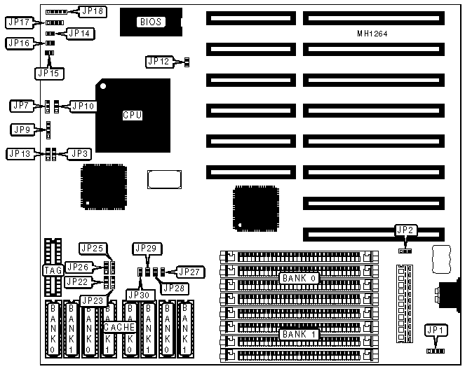
External battery |
JP1 |
Turbo LED |
JP16 |
|
Reset switch |
JP14 |
Speaker |
JP17 |
|
Turbo switch |
JP15 |
Power LED & keylock |
JP18 |
|
USER CONFIGURABLE SETTINGS | |||
|
Function |
Jumper |
Position | |
| » |
CMOS memory normal operation |
JP2 |
pins 1 & 2 closed |
|
CMOS memory clear |
JP2 |
pins 2 & 3 closed | |
| » |
CPU speed (external) select 16/20/25/33/40MHz |
JP3 |
pins 1 & 2 closed |
|
CPU speed (external) select 50MHz |
JP3 |
pins 2 & 3 closed | |
| » |
Monitor type select color |
JP12 |
open |
|
Monitor type select monochrome |
JP12 |
closed | |
|
CPU TYPE CONFIGURATION | |||
|
Jumper |
JP7 |
JP9 |
JP13 |
|
80486DX2 |
pins 1 & 2 closed |
pins 1 & 2 and 3 & 4 closed |
pins 1 & 2 closed |
|
80486DX |
pins 1 & 2 closed |
pins 1 & 2 and 3 & 4 closed |
pins 1 & 2 closed |
|
80487SX |
pins 2 & 3 closed |
pins 1 & 2 and 3 & 4 closed |
pins 1 & 2 closed |
|
80486SX |
open |
pins 2 & 3 closed |
pins 2 & 3 closed |
|
DRAM CONFIGURATION | ||
|
Size |
Bank 0 |
Bank 1 |
|
1MB |
(4) 256K x 9 |
NONE |
|
2MB |
(4) 256K x 9 |
(4) 256K x 9 |
|
4MB |
(4) 1M x 9 |
NONE |
|
5MB |
(4) 256K x 9 |
(4) 1M x 9 |
|
8MB |
(4) 1M x 9 |
(4) 1M x 9 |
|
16MB |
(4) 4M x 9 |
NONE |
|
20MB |
(4) 1M x 9 |
(4) 4M x 9 |
|
32MB |
(4) 4M x 9 |
(4) 4M x 9 |
|
64MB |
(4) 16M x 9 |
NONE |
|
128MB |
(4) 16M x 9 |
(4) 16M x 9 |
|
SRAM JUMPER CONFIGURATION | ||||
|
Jumper |
32KB |
64KB |
128KB |
256KB |
|
JP22 |
pins 2 & 3 closed |
pins 2 & 3 closed |
pins 2 & 3 closed |
pins 1 & 2 closed |
|
JP23 |
pins 2 & 3 closed |
pins 2 & 3 closed |
pins 1 & 2 closed |
pins 2 & 3 closed |
|
JP25 |
pins 1 & 2 closed |
pins 2 & 3 closed |
pins 2 & 3 closed |
pins 2 & 3 closed |
|
JP26 |
pins 2 & 3 closed |
pins 1 & 2 closed |
pins 2 & 3 closed |
pins 2 & 3 closed |
|
JP27 |
closed |
open |
open |
open |
|
JP28 |
open |
closed |
open |
open |
|
JP29 |
open |
open |
closed |
open |
|
JP30 |
open |
open |
open |
closed |
|
SRAM CONFIGURATION | |||
|
Size |
Cache SRAM |
Location |
TAG |
|
32KB |
(4) 8K x 8 |
Bank 0 |
(1) 8K x 8 |
|
64KB |
(8) 8K x 8 |
Banks 0 & 1 |
(1) 8K x 8 |
|
128KB |
(4) 32K x 8 |
Bank 0 |
(1) 32K x 8 |
|
256KB |
(8) 32K x 8 |
Banks 0 & 1 |
(1) 32K x 8 |