ATEN RESEARCH, INC.
486 LOCAL BUS MAINBOARD
|
Processor |
80486SX/80486DX/80486DX2 |
|
Processor Speed |
20/25/33/50(internal)/50/66(internal)MHz |
|
Chip Set |
OPTI |
|
Max. Onboard DRAM |
64MB |
|
Cache |
64/256KB |
|
BIOS |
AMI |
|
Dimensions |
330mm x 218mm |
|
I/O Options |
32-bit local bus card slot |
|
NPU Options |
4167 |
|
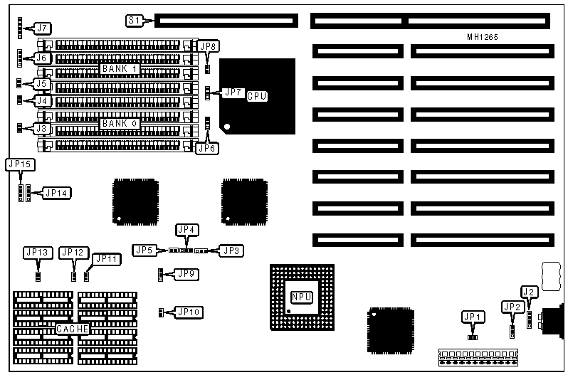
CONNECTIONS | |||
|
Purpose |
Location |
Purpose |
Location |
|
External battery |
J2 pins 1 & 4 |
Speaker |
J6 |
|
Turbo switch |
J3 |
Power LED & keylock |
J7 |
|
Reset switch |
J4 |
32-bit local bus card |
S1 |
|
Turbo LED |
J5 | ||
|
USER CONFIGURABLE SETTINGS | |||
|
Function |
Jumper |
Position | |
| » |
Battery type select internal |
J2 |
pins 2 & 3 closed |
|
Battery type select external |
J2 |
pins 1 & 4 connected | |
| » |
Monitor type select color |
JP1 |
closed |
|
Monitor type select monochrome |
JP1 |
open | |
| » |
CMOS memory normal operation |
JP2 |
pins 1 & 2 closed |
|
CMOS memory clear |
JP2 |
pins 2 & 3 closed | |
| » |
VGA card type select ISA |
JP3 JP4 |
pins 1 & 2 closed pins 1 & 2 closed |
|
VGA card type select local bus with ET 4000 chipset |
JP3 JP4 |
pins 2 & 3 closed pins 2 & 3 closed | |
|
VGA card type select local bus with S3 chipset |
JP3 JP4 |
pins 2 & 3 closed pins 1 & 2 closed | |
| » |
I/O Bus speed select ATCLK/4 |
JP5 |
open |
|
I/O Bus speed select ATCLK/6 |
JP5 |
closed | |
| » |
CPU speed select iOSC/2 |
JP9 |
pins 2 & 3 closed |
|
CPU speed select iOSC/1 |
JP9 |
pins 1 & 2 closed | |
|
CPU CONFIGURATION | |||
|
CPU Type |
JP6 |
JP7 |
JP8 |
|
80486DX2 |
pins 1 & 2 closed |
pins 2 & 3 closed |
closed |
|
80486DX |
pins 1 & 2 closed |
pins 2 & 3 closed |
closed |
|
80486SX |
pins 2 & 3 closed |
open |
open |
|
SRAM JUMPER CONFIGURATION | ||||
|
Size |
JP10 |
JP11 |
JP12 |
JP13 |
|
64KB |
open |
open |
open |
open |
|
256KB |
closed |
closed |
open |
closed |
|
SRAM CONFIGURATION | |||
|
Size |
Cache SRAM |
TAG (U46) |
TAG (U47) |
|
64KB |
(8) 8K x 8 |
(1) 64K x 1 |
(1) 8K x 8 |
|
256KB |
(8) 32K x 8 |
(1) 64K x 1 |
(1) 32K x 8 |
|
Note:Locations of U46 and U47 are unknown. | |||
|
DRAM CONFIGURATION | ||||
|
Size |
Bank 0 |
Bank 1 |
Bank 2 |
Bank 3 |
|
1MB |
(4) 256K x 9 |
NONE |
NONE |
NONE |
|
2MB |
(4) 256K x 9 |
(4) 256K x 9 |
NONE |
NONE |
|
3MB |
(4) 256K x 9 |
(4) 256K x 9 |
(4) 256K x 9 |
NONE |
|
4MB |
(4) 256K x 9 |
(4) 256K x 9 |
(4) 256K x 9 |
(4) 256K x 9 |
|
5MB |
(4) 1M x 9 |
(4) 256K x 9 |
NONE |
NONE |
|
6MB |
(4) 256K x 9 |
(4) 256K x 9 |
(4) 1M x 9 |
NONE |
|
7MB |
(4) 256K x 9 |
(4) 256K x 9 |
(4) 256K x 9 |
(4) 1M x 9 |
|
8MB |
(4) 1M x 9 |
(4) 1M x 9 |
NONE |
NONE |
|
9MB |
(4) 256K x 9 |
(4) 1M x 9 |
(4) 1M x 9 |
NONE |
|
10MB |
(4) 256K x 9 |
(4) 256K x 9 |
(4) 1M x 9 |
(4) 1M x 9 |
|
12MB |
(4) 1M x 9 |
(4) 1M x 9 |
(4) 1M x 9 |
NONE |
|
13MB |
(4) 256K x 9 |
(4) 1M x 9 |
(4) 1M x 9 |
(4) 1M x 9 |
|
16MB |
(4) 1M x 9 |
(4) 1M x 9 |
(4) 1M x 9 |
(4) 1M x 9 |
|
16MB |
(4) 4M x 9 |
NONE |
NONE |
NONE |
|
20MB |
(4) 1M x 9 |
(4) 4M x 9 |
NONE |
NONE |
|
24MB |
(4) 1M x 9 |
(4) 1M x 9 |
(4) 4M x 9 |
NONE |
|
28MB |
(4) 1M x 9 |
(4) 1M x 9 |
(4) 1M x 9 |
(4) 4M x 9 |
|
32MB |
(4) 4M x 9 |
(4) 4M x 9 |
NONE |
NONE |
|
36MB |
(4) 1M x 9 |
(4) 4M x 9 |
(4) 4M x 9 |
NONE |
|
40MB |
(4) 1M x 9 |
(4) 1M x 9 |
(4) 4M x 9 |
(4) 4M x 9 |
|
48MB |
(4) 4M x 9 |
(4) 4M x 9 |
(4) 4M x 9 |
NONE |
|
52MB |
(4) 1M x 9 |
(4) 4M x 9 |
(4) 4M x 9 |
(4) 4M x 9 |
|
64MB |
(4) 4M x 9 |
(4) 4M x 9 |
(4) 4M x 9 |
(4) 4M x 9 |