CSS LABORATORIES, INC.
PREFERRED 433GE (Rev. B)
|
Processor |
80486DX/80486DX2 |
|
Processor Speed |
25/33/50(internal)/66(internal)MHz |
|
Chip Set |
C & T |
|
Max. Onboard DRAM |
24MB |
|
SRAM Cache |
32/256KB |
|
BIOS |
Award/Phoenix |
|
Dimensions |
355mm x 304mm |
|
I/O Options |
32-bit external memory card slot, 32-bit external cache card slot 32-bit local video card slot, auxiliary keyboard, IDE interface floppy drive interface, parallel port, serial port (2) |
|
NPU Options |
4167 |
|
CONNECTIONS |
|||
|
Purpose |
Location |
Purpose |
Location |
|
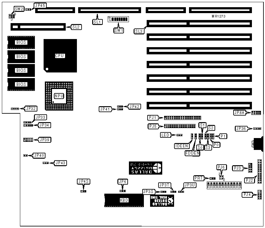
Front panel switches & LEDs |
JP39 |
IDE interface |
PJ1 |
|
External hard drive access LED |
JP40 |
Parallel port |
PJ2 |
|
Auxiliary keyboard |
JP8A |
Serial port 1 |
PJ3 |
|
Reset switch |
JP32 pins 1 & 2 |
Serial port 2 |
PJ4 |
|
Turbo LED |
JP32 pins 3 & 4 |
Floppy drive interface |
PJ5 |
|
Speaker |
JP33 |
32-bit external memory card |
SL1 |
|
Power LED & keylock |
JP34 |
32-bit external cache card |
SL2 |
|
External battery |
JP36 |
32-bit MaxGraphics video card |
SL3 |
|
IDE interface LED |
LED |
|
|
|
USER CONFIGURABLE SETTINGS |
|||
|
Function |
Jumper/Switch |
Position |
|
|
» |
Floppy drive interface enabled |
FDDEN |
pins 2 & 3 closed |
|
|
Floppy drive interface disabled |
FDDEN |
pins 1 & 2 closed |
|
» |
IDE interface enabled |
IDEEN |
pins 2 & 3 closed |
|
|
IDE interface disabled |
IDEEN |
pins 1 & 2 closed |
|
» |
Factory configured - do not alter |
JP3S |
pins 2 & 3 closed |
|
» |
Factory configured - do not alter |
JP3T |
pins 2 & 3 closed |
|
» |
Factory configured - do not alter |
JP3U |
pins 2 & 3 closed |
|
» |
Factory configured - do not alter |
JP4S |
pins 1 & 2 closed |
|
|
BIOS type select Award |
JP6 |
pins 1 & 2 closed |
|
|
BIOS type select Phoenix |
JP6 |
pins 2 & 3 closed |
|
» |
Factory configured - do not alter |
JP41 |
unknown |
|
» |
Factory configured - do not alter |
JP42 |
pins 2 & 3 closed |
|
» |
Factory configured - do not alter |
JP43 |
unknown |
|
» |
External cache disabled |
JP45 |
pins 2 & 3 closed |
|
|
External cache enabled |
JP45 |
pins 1 & 2 closed |
|
» |
Cacheable address from 768 to 895KB disabled |
SW1/Switch 1 |
open |
|
|
Cacheable address from 768 to 895KB enabled |
SW1/Switch 1 |
closed |
|
» |
Cacheable address from 896 to 1024KB disabled |
SW1/Switch 2 |
open |
|
|
Cacheable address from 896 to 1024KB enabled |
SW1/Switch 2 |
closed |
|
» |
Cacheable address from 0 to 640KB & 1 to 64MB enabled |
SW1/Switch 3 |
closed |
|
|
Cacheable address from 0 to 640KB & 1 to 64MB disabled |
SW1/Switch 3 |
open |
|
|
NPU error override enabled |
SW1/Switch 4 |
closed |
|
|
NPU error override disabled |
SW1/Switch 4 |
open |
|
|
Monitor type select color |
SW1/Switch 5 |
closed |
|
|
Monitor type select monochrome |
SW1/Switch 5 |
open |
|
» |
Factory configured - do not alter |
SW1/Switch 6 |
unknown |
|
» |
Factory configured - do not alter |
SW1/Switch 7 |
unknown |
|
» |
Factory configured - do not alter |
SW1/Switch 8 |
unknown |
|
» |
Factory configured - do not alter |
SW2 |
pins 3 & 4 closed |
|
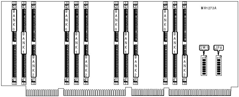
DRAM SWITCH (SW1) CONFIGURATION |
||||||||
|
Size |
Switch 1 |
Switch 2 |
Switch 3 |
Switch 4 |
Switch 5 |
Switch 6 |
Switch 7 |
Switch 8 |
|
4MB |
closed |
open |
closed |
open |
open |
N/A |
N/A |
open |
|
8MB |
closed |
open |
closed |
open |
open |
N/A |
N/A |
open |
|
8MB |
open |
closed |
closed |
open |
open |
N/A |
N/A |
open |
|
12MB |
closed |
open |
closed |
open |
open |
N/A |
N/A |
open |
|
12MB |
open |
closed |
closed |
open |
open |
N/A |
N/A |
open |
|
16MB |
open |
closed |
closed |
open |
open |
N/A |
N/A |
open |
|
16MB |
open |
closed |
open |
closed |
open |
N/A |
N/A |
open |
|
16MB |
closed |
open |
closed |
open |
open |
N/A |
N/A |
closed |
|
20MB |
closed |
open |
closed |
open |
open |
N/A |
N/A |
open |
|
24MB |
open |
closed |
open |
closed |
open |
N/A |
N/A |
open |
|
DRAM SWITCH (JP8) CONFIGURATION |
||||||||
|
Size |
Switch 1 |
Switch 2 |
Switch 3 |
Switch 4 |
Switch 5 |
Switch 6 |
Switch 7 |
Switch 8 |
|
4MB |
closed |
open |
open |
open |
open |
open |
open |
open |
|
8MB |
closed |
open |
open |
open |
closed |
open |
open |
open |
|
8MB |
closed |
closed |
open |
open |
open |
open |
open |
open |
|
12MB |
closed |
open |
closed |
open |
closed |
open |
closed |
open |
|
12MB |
closed |
closed |
closed |
open |
open |
open |
open |
open |
|
16MB |
closed |
closed |
closed |
closed |
open |
open |
open |
open |
|
16MB |
closed |
closed |
closed |
closed |
open |
open |
open |
open |
|
16MB |
closed |
open |
open |
open |
open |
open |
open |
open |
|
20MB |
closed |
closed |
closed |
closed |
closed |
open |
open |
open |
|
24MB |
closed |
closed |
closed |
closed |
closed |
open |
closed |
open |
|
DRAM CONFIGURATION |
|||
|
Size |
Bank 0 |
Bank 1 |
Bank 2 |
|
4MB |
(4) 256K x 36 |
NONE |
NONE |
|
8MB |
(4) 256K x 36 |
(4) 256K x 36 |
NONE |
|
8MB |
(4) 512K x 36 |
NONE |
NONE |
|
12MB |
(4) 256K x 36 |
(4) 256K x 36 |
(4) 256K x 36 |
|
12MB |
(4) 512K x 36 |
(4) 256K x 36 |
NONE |
|
16MB |
(4) 512K x 36 |
(4) 256K x 36 |
(4) 256K x 36 |
|
16MB |
(4) 512K x 36 |
(4) 512K x 36 |
NONE |
|
16MB |
(4) 1M x 36 |
NONE |
NONE |
|
20MB |
(4) 512K x 36 |
(4) 512K x 36 |
(4) 256K x 36 |
|
24MB |
(4) 512K x 36 |
(4) 512K x 36 |
(4) 512K x 36 |
|
SERIAL PORT 1 (PJ3) CONFIGURATION |
|||||
|
COM |
Interrupt |
I/O Address |
Jumper PJ6 |
S0 |
S1 |
|
COM 2 |
IRQ3 |
2F8h |
pins 1 & 3 |
pins 1 & 2 |
pins 2 & 3 |
|
COM 1 |
IRQ4 |
3F8h |
pins 1 & 2 |
pins 2 & 3 |
pins 2 & 3 |
|
Disabled |
N/A |
N/A |
N/A |
pins 1 & 2 |
pins 1 & 2 |
|
Note: Pins designated should be in the closed position. |
|||||
|
SERIAL PORT 2 (PJ4) CONFIGURATION |
|||||
|
COM |
Interrupt |
I/O Address |
Jumper PJ6 |
S2 |
S3 |
|
COM 1 |
IRQ4 |
3F8h |
pins 2 & 4 |
pins 1 & 2 |
pins 2 & 3 |
|
COM 2 |
IRQ3 |
2F8h |
pins 3 & 4 |
pins 2 & 3 |
pins 2 & 3 |
|
Disabled |
N/A |
N/A |
N/A |
pins 1 & 2 |
pins 1 & 2 |
|
Note: Pins designated should be in the closed position. |
|||||
|
PARALLEL PORT 1 (PJ2) CONFIGURATION |
|||||
|
LPT |
Interrupt |
I/O Address |
Jumper P0 |
Jumper P1 |
Jumper PRT |
|
LPT 1 |
IRQ7 |
3F8h |
pins 1 & 2 |
pins 2 & 3 |
pins 2 & 3 |
|
LPT 2 |
IRQ5 |
2F8h |
pins 2 & 3 |
pins 2 & 3 |
pins 1 & 2 |
|
LPT 3 |
IRQ7 |
3BCh |
pins 2 & 3 |
pins 1 & 2 |
pins 2 & 3 |
|
Disabled |
N/A |
N/A |
pins 1 & 2 |
pins 1 & 2 |
N/A |
|
Note: Pins designated should be in the closed position. |
|||||