CSS LABORATORIES, INC.
PREFERRED 486 MGE/VL
|
Processor |
80486DX/80486DX2/Pentium Overdrive |
|
Processor Speed |
25/33/50(internal)/50/66(internal)MHz |
|
Chip Set |
SIS |
|
Max. Onboard DRAM |
256MB (128MB on CPU module) |
|
Cache |
512KB (on CPU module) |
|
BIOS |
AMI |
|
Dimensions |
330mm x 218mm |
|
I/O Options |
CPU module slot, 32-bit VESA local bus slots (2) |
|
NPU Options |
None |
|
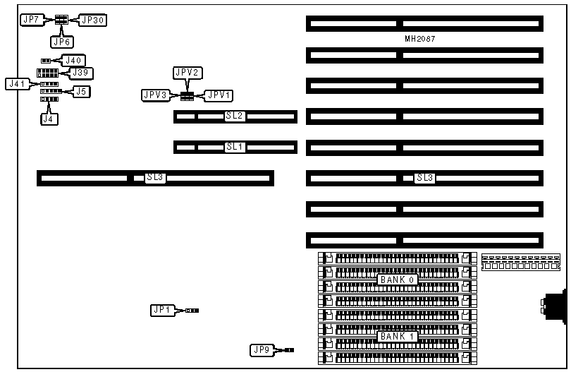
CONNECTIONS | |||
|
Purpose |
Location |
Purpose |
Location |
|
Speaker |
J4 |
Reset/Turbo switch |
J41 |
|
Power LED & keylock |
J5 |
32-bit VESA Local bus slots |
SL1 & SL2 |
|
Equipment panel connector |
J39 |
CPU module slot |
SL3 |
|
IDE interface LED |
J40 | ||
|
USER CONFIGURABLE SETTINGS | |||
|
Function |
Jumper |
Position | |
|
» |
Monitor type select monochrome |
JP9 |
Closed |
|
Monitor type select color |
JP9 |
Open | |
|
» |
Factory configured - do not alter |
JP30 |
Open |
|
DRAM CONFIGURATION | ||||
|
Size |
Bank 0 |
Bank 1 |
Bank 2 |
Bank 3 |
|
4MB |
(4) 1M x 9 |
NONE |
NONE |
NONE |
|
8MB |
(4) 1M x 9 |
(4) 1M x 9 |
NONE |
NONE |
|
12MB |
(4) 1M x 9 |
(4) 1M x 9 |
(4) 1M x 9 |
NONE |
|
16MB |
(4) 1M x 9 |
(4) 1M x 9 |
(4) 1M x 9 |
(4) 1M x 9 |
|
16MB |
(4) 4M x 9 |
NONE |
NONE |
NONE |
|
20MB |
(4) 1M x 9 |
(4) 4M x 9 |
NONE |
NONE |
|
24MB |
(4) 1M x 9 |
(4) 1M x 9 |
(4) 4M x 9 |
NONE |
|
24MB |
(4) 1M x 9 |
(4) 4M x 9 |
(4) 1M x 9 |
NONE |
|
28MB |
(4) 1M x 9 |
(4) 1M x 9 |
(4) 4M x 9 |
(4) 1M x 9 |
|
28MB |
(4) 1M x 9 |
(4) 4M x 9 |
(4) 1M x 9 |
(4) 1M x 9 |
|
32MB |
(4) 4M x 9 |
(4) 4M x 9 |
NONE |
NONE |
|
36MB |
(4) 1M x 9 |
(4) 4M x 9 |
(4) 4M x 9 |
NONE |
|
36MB |
(4) 4M x 9 |
(4) 4M x 9 |
(4) 1M x 9 |
NONE |
|
40MB |
(4) 1M x 9 |
(4) 1M x 9 |
(4) 4M x 9 |
(4) 4M x 9 |
|
40MB |
(4) 1M x 9 |
(4) 4M x 9 |
(4) 4M x 9 |
(4) 1M x 9 |
|
40MB |
(4) 4M x 9 |
(4) 4M x 9 |
(4) 1M x 9 |
(4) 1M x 9 |
|
48MB |
(4) 4M x 9 |
(4) 4M x 9 |
(4) 4M x 9 |
NONE |
|
52MB |
(4) 1M x 9 |
(4) 4M x 9 |
(4) 4M x 9 |
(4) 4M x 9 |
|
52MB |
(4) 4M x 9 |
(4) 4M x 9 |
(4) 4M x 9 |
(4) 1M x 9 |
|
64MB |
(4) 4M x 9 |
(4) 4M x 9 |
(4) 4M x 9 |
(4) 4M x 9 |
|
64MB |
(4) 16M x 9 |
NONE |
NONE |
NONE |
|
128MB |
(4) 16M x 9 |
(4) 16M x 9 |
NONE |
NONE |
|
196MB |
(4) 16M x 9 |
(4) 16M x 9 |
(4) 16M x 9 |
NONE |
|
256MB |
(4) 16M x 9 |
(4) 16M x 9 |
(4) 16M x 9 |
(4) 16M x 9 |
|
Note: Banks 2 & 3 are located on the CPU module board. | ||||
|
CPU SPEED CONFIGURATION | |||
|
Speed |
JP1 |
JP6 |
JP7 |
|
25MHz |
pins 1 & 2 closed |
Open |
Open |
|
33MHz |
pins 1 & 2 closed |
Open |
Closed |
|
50iMHz |
pins 1 & 2 closed |
Closed |
Closed |
|
66iMHz |
pins 1 & 2 closed |
Open |
Closed |
|
VESA BUS SPEED CONFIGURATION | |
|
CPU speed |
JPV3 |
|
<=33MHz |
Open |
|
> 33MHz |
Closed |
|
VESA WAIT STATE CONFIGURATION | ||
|
Wait states |
JPV1 |
JPV2 |
|
0 wait states |
Open |
Open |
|
1 wait state |
Closed |
Closed |
|
EQUIPMENT PANEL CONFIGURATION | |
|
Description |
J39 |
|
Ground |
pin 1 |
|
Power |
pin 2 |
|
Hard drive LED |
pin 3 |
|
Not used |
pin 4 |
|
Power |
pin 5 |
|
Ground |
pin 6 |
|
Turbo LED |
pin 7 |
|
Keyboard inhibit |
pin 8 |
|
Power |
pin 9 |
|
Reset button |
pin 10 |