CSS LABORATORIES, INC.
PREFERRED 462 PCI/VL ESP, MB-4862
|
Processor |
80486SX/80487SX/CX486M7/80486DX/80486DX2/80486DX4/ Pentium Overdrive |
|
Processor Speed |
8/16/25/33/40/50(internal)/50/66(internal)100(internal)MHz |
|
Chip Set |
OPTI |
|
Max. Onboard DRAM |
128MB |
|
Cache |
64/128/256KB |
|
BIOS |
Award |
|
Dimensions |
330mm x 218mm |
|
I/O Options |
32-bit VESA local bus slots (2), 32-bit PCI slots (3) |
|
NPU Options |
None |
|
CONNECTIONS |
|||
|
Purpose |
Location |
Purpose |
Location |
|
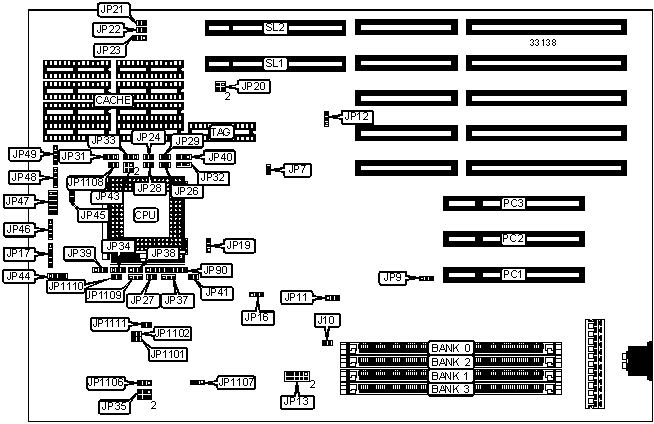
Power LED & keylock |
JP17 |
Turbo switch |
JP48 pins 3 & 4 |
|
IDE interface LED |
JP45 |
External battery |
JP49 |
|
Speaker |
JP46 |
32-bit PCI slots |
PC1 - PC3 |
|
Front panel connector |
JP47 |
32-bit VESA local bus slots |
SL1 & SL2 |
|
Reset switch |
JP48 pins 1 & 2 |
|
|
|
USER CONFIGURABLE SETTINGS |
|||
|
Function |
Jumper |
Position |
|
|
» |
Factory configured - do not alter |
J10 |
N/A |
|
» |
Factory configured - do not alter |
JP7 |
N/A |
|
» |
Local bus type select synchronous |
JP9 |
pins 1 & 2 closed |
|
|
Local bus type select asynchronous |
JP9 |
pins 2 & 3 closed |
|
|
PCI bus type select synchronous |
JP11 |
pins 2 & 3 closed |
|
|
PCI bus type select asynchronous |
JP11 |
pins 1 & 2 closed |
|
» |
Factory configured - do not alter |
JP12 |
N/A |
|
» |
Factory configured - do not alter |
JP13 |
N/A |
|
» |
Factory configured - do not alter |
JP19 |
N/A |
|
» |
Factory configured - do not alter |
JP20 |
N/A |
|
» |
Factory configured - do not alter |
JP23 |
N/A |
|
» |
Factory configured - do not alter |
JP26 |
N/A |
|
» |
Factory configured - do not alter |
JP27 |
N/A |
|
» |
Factory configured - do not alter |
JP40 |
N/A |
|
» |
Factory configured - do not alter |
JP90 |
N/A |
|
» |
Factory configured - do not alter |
JP1106 |
N/A |
|
» |
Factory configured - do not alter |
JP1108 |
N/A |
|
» |
Factory configured - do not alter |
JP1109 |
N/A |
|
» |
Factory configured - do not alter |
JP1111 |
N/A |
|
DRAM CONFIGURATION |
||||
|
Size |
Bank 0 |
Bank 1 |
Bank 2 |
Bank 3 |
|
1MB |
(1) 256K x 36 |
NONE |
NONE |
NONE |
|
2MB |
(1) 256K x 36 |
(1) 256K x 36 |
NONE |
NONE |
|
2MB |
(1) 512K x 36 |
NONE |
NONE |
NONE |
|
3MB |
(1) 256K x 36 |
(1) 256K x 36 |
(1) 256K x 36 |
NONE |
|
4MB |
(1) 256K x 36 |
(1) 256K x 36 |
(1) 256K x 36 |
(1) 256K x 36 |
|
4MB |
(1) 512K x 36 |
(1) 512K x 36 |
NONE |
NONE |
|
4MB |
(1) 1M x 36 |
NONE |
NONE |
NONE |
|
6MB |
(1) 512K x 36 |
(1) 512K x 36 |
(1) 512K x 36 |
NONE |
|
8MB |
(1) 512K x 36 |
(1) 512K x 36 |
(1) 512K x 36 |
(1) 512K x 36 |
|
8MB |
(1) 1M x 36 |
(1) 1M x 36 |
NONE |
NONE |
|
8MB |
(1) 2M x 36 |
NONE |
NONE |
NONE |
|
12MB |
(1) 1M x 36 |
(1) 1M x 36 |
(1) 1M x 36 |
NONE |
|
16MB |
(1) 1M x 36 |
(1) 1M x 36 |
(1) 1M x 36 |
(1) 1M x 36 |
|
16MB |
(1) 2M x 36 |
(1) 2M x 36 |
NONE |
NONE |
|
16MB |
(1) 4M x 36 |
NONE |
NONE |
NONE |
|
24MB |
(1) 2M x 36 |
(1) 2M x 36 |
(1) 2M x 36 |
NONE |
|
32MB |
(1) 2M x 36 |
(1) 2M x 36 |
(1) 2M x 36 |
(1) 2M x 36 |
|
32MB |
(1) 4M x 36 |
(1) 4M x 36 |
NONE |
NONE |
|
32MB |
(1) 8M x 36 |
NONE |
NONE |
NONE |
|
48MB |
(1) 4M x 36 |
(1) 4M x 36 |
(1) 4M x 36 |
NONE |
|
64MB |
(1) 4M x 36 |
(1) 4M x 36 |
(1) 4M x 36 |
(1) 4M x 36 |
|
64MB |
(1) 8M x 36 |
(1) 8M x 36 |
NONE |
NONE |
|
DRAM CONFIGURATION (CON'T) |
||||
|
Size |
Bank 0 |
Bank 1 |
Bank 2 |
Bank 3 |
|
64MB |
(1) 16M x 36 |
NONE |
NONE |
NONE |
|
96MB |
(1) 8M x 36 |
(1) 8M x 36 |
(1) 8M x 36 |
NONE |
|
128MB |
(1) 8M x 36 |
(1) 8M x 36 |
(1) 8M x 36 |
(1) 8M x 36 |
|
128MB |
(1) 16M x 36 |
(1) 16M x 36 |
NONE |
NONE |
|
CACHE CONFIGURATION |
|||
|
Size |
Bank 0 |
Bank 1 |
TAG |
|
64KB |
(4) 8K x 8 |
(4) 8K x 8 |
(1) 8K x 8 or (1) 32K x 8 |
|
128KB |
(4) 32K x 8 |
NONE |
(1) 8K x 8 |
|
256KB |
(4) 32K x 8 |
(4) 32K x 8 |
(1) 32K x 8 |
|
Note: The orientation of Bank 0 & 1 is unidentified. |
|||
|
CACHE JUMPER CONFIGURATION |
||||
|
Size |
jp24 |
jp29 |
JP32 |
JP33 |
|
64KB |
Open |
Open |
pins 2 & 3 closed |
pins 2 & 3 closed |
|
128KB |
Open |
Closed |
pins 1 & 2 closed |
pins 1 & 2 closed |
|
256KB |
Closed |
Closed |
pins 2 & 3 closed |
pins 2 & 3 closed |
|
CPU TYPE CONFIGURATION |
||||||
|
Type |
JP17 |
JP28 |
JP34 |
JP37 |
JP38 |
JP39 |
|
80486SX |
N/A |
Open |
Open |
N/A |
N/A |
1 & 2 |
|
80487SX |
N/A |
Open |
1 & 2 |
2 & 3 |
1 & 2 |
1 & 2 |
|
CX486M7 |
N/A |
Closed |
2 & 3 |
N/A |
2 & 3 |
2 & 3 |
|
80486DX |
Closed |
Open |
2 & 3 |
2 & 3 |
1 & 2 |
1 & 2 |
|
80486DX2 |
Closed |
Open |
2 & 3 |
2 & 3 |
1 & 2 |
1 & 2 |
|
80486DX4 |
Closed |
Open |
2 & 3 |
2 & 3 |
1 & 2 |
2 & 3 |
|
P24T |
N/A |
Open |
N/A |
N/A |
N/A |
2 & 3 |
|
Note: Pins designated should be in the closed position. |
||||||
|
CPU TYPE CONFIGURATION (CON'T) |
|||||
|
Type |
JP41 |
JP43 |
JP44 |
JP1101 |
JP1102 |
|
80486SX |
N/A |
N/A |
2 & 3 |
Closed |
Closed |
|
80487SX |
N/A |
N/A |
1 & 2, 3 & 4 |
Closed |
Closed |
|
CX486M7 |
N/A |
2 & 4 |
N/A |
Open |
Open |
|
80486DX |
Closed |
N/A |
1 & 2, 3 & 4 |
Closed |
Closed |
|
80486DX2 |
Closed |
N/A |
1 & 2, 3 & 4 |
Closed |
Closed |
|
80486DX4 |
Closed |
N/A |
1 & 2, 3 & 4 |
Open |
Open |
|
P24T |
N/A |
N/A |
N/A |
Closed |
Closed |
|
Note: Pins designated should be in the closed position. |
|||||
|
CPU SPEED CONFIGURATION |
|
|
Speed |
JP35 |
|
8MHz |
Open |
|
16MHz |
pins 3 & 4 closed |
|
25MHz |
pins 1 & 2 closed |
|
33MHz |
pins 1 & 2, 5 & 6 closed |
|
40MHz |
pins 1 & 2, 3 & 4 closed |
|
50iMHz |
pins 1 & 2 closed |
|
50MHz |
pins 1 & 2, 3 & 4, 5 & 6 closed |
|
66iMHz |
pins 1 & 2, 5 & 6 closed |
|
100iMHz |
pins 1 & 2, 5 & 6 closed |
|
CPU SPEED CONFIGURATION (CYRIX ONLY) |
|
|
Setting |
JP1110 |
|
Internal clock doubled |
Closed |
|
Internal clock standard |
Open |
|
VL BUS WAIT STATE CONFIGURATION |
|
|
Wait states |
JP21 |
|
0 wait states |
Open |
|
1 wait state |
Closed |
|
VL BUS SPEED CONFIGURATION |
||
|
CPU speed |
JP22 |
JP31 |
|
<= 33MHz |
Open |
pins 1 & 2 closed |
|
> 33MHz |
pins 1 & 2 closed |
Open |
|
FLASH BIOS CONFIGURATION |
|||
|
Setting |
JP16 |
JP1107 |
|
|
» |
Disabled |
pins 2 & 3 closed |
pins 1 & 2 closed |
|
» |
Enabled |
pins 1 & 2 closed |
pins 2 & 3 closed |