DIGITAL EQUIPMENT CORPORATION
DIGITAL 21164
|
Processor |
Alpha |
|
Processor Speed |
266/300/333MHz |
|
Chip Set |
DEC |
|
Video Chip Set |
None |
|
Maximum Onboard Memory |
512MB |
|
Maximum Video Memory |
None |
|
Cache |
2048/4096/8192KB |
|
BIOS |
Unidentified |
|
Dimensions |
332mm x 307mm |
|
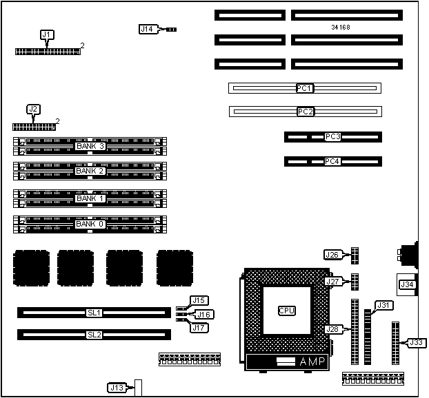
I/O Options |
64-bit PCI slots (2), 32-bit PCI slots (2), floppy drive interface, IDE interface, parallel port, PS/2 mouse port, serial ports (2), cache slots (2) |
|
NPU Options |
None |
|
CONNECTIONS | |||
|
Purpose |
Location |
Purpose |
Location |
|
Chassis fan power |
J2/pins 3 & 5 |
Serial port 1 |
J27 |
|
Chassis fan power |
J2/pins 7 & 9 |
IDE interface |
J28 |
|
Halt connector |
J2/pins 8 & 10 |
Floppy drive interface |
J31 |
|
Chassis fan power |
J2/pins 11 & 13 |
Parallel port |
J33 |
|
Reset switch |
J2/pins 12 & 14 |
PS/2 mouse port |
J34 |
|
IDE interface LED |
J2/pins 15 & 17 |
64-bit PCI slots |
PC1 & PC2 |
|
Keylock |
J2/pins 18 & 20 |
32-bit PCI slots |
PC3 & PC4 |
|
Speaker |
J2/pins 19,21,23,25 |
Cache slot |
SL1 |
|
Serial port 2 |
J26 |
Cache slot |
SL2 |
|
USER CONFIGURABLE SETTINGS | |||
|
Function |
Label |
Position | |
|
» |
Factory configured - do not alter |
J1/pins 9 & 10 |
N/A |
|
» |
SROM test disabled |
J1/pins 23 & 24 |
Open |
|
SROM test enabled |
J1/pins 23 & 24 |
Closed | |
|
» |
Loaded image select alternate images loaded |
J1/pins 25 & 26 |
Closed |
|
Loaded image select first image loaded |
J1/pins 25 & 26 |
Open | |
|
» |
Cache speed select nominal read speed |
J1/pins 29 & 30 |
Open |
|
Cache speed select read speed 1 cycle faster |
J1/pins 29 & 30 |
Closed | |
|
» |
Factory configured - do not alter |
J1/pins 31 & 32 |
N/A |
|
» |
Factory configured - do not alter |
J1/pins 33 & 34 |
N/A |
|
» |
Factory configured - do not alter |
J1/pins 35 & 36 |
N/A |
|
» |
Factory configured - do not alter |
J1/pins 37 & 38 |
N/A |
|
» |
Factory configured - do not alter |
J1/pins 39 & 40 |
N/A |
|
» |
SROM test connector |
J13 |
N/A |
|
» |
Flash BIOS write protect disabled |
J14 |
Pins 2 & 3 closed |
|
Flash BIOS write protect enabled |
J14 |
Pins 1 & 2 closed | |
|
DRAM CONFIGURATION | ||||
|
Size |
Bank 0 |
Bank 1 |
Bank 2 |
Bank 3 |
|
32MB |
(2) 1M x 36 |
(2) 1M x 36 |
(2) 1M x 36 |
(2) 1M x 36 |
|
64MB |
(2) 2M x 36 |
(2) 2M x 36 |
(2) 2M x 36 |
(2) 2M x 36 |
|
128MB |
(2) 4M x 36 |
(2) 4M x 36 |
(2) 4M x 36 |
(2) 4M x 36 |
|
256MB |
(2) 8M x 36 |
(2) 8M x 36 |
(2) 8M x 36 |
(2) 8M x 36 |
|
512MB |
(2) 16M x 36 |
(2) 16M x 36 |
(2) 16M x 36 |
(2) 16M x 36 |
|
CACHE CONFIGURATION | ||
|
Size |
SL1 |
SL2 |
|
2MB |
2MB |
None |
|
4MB |
4MB |
None |
|
8MB |
4MB |
4MB |
|
Note: The sizes of the cache modules are unidentified. | ||
|
CACHE JUMPER CONFIGURATION | |||
|
Size |
J1/pins 11 & 12 |
J1/pins 13 & 14 |
J1/pins 15 & 16 |
|
2MB |
Closed |
Open |
Open |
|
4MB |
Open |
Closed |
Closed |
|
8MB |
Open |
Closed |
Open |
|
CACHE ADDRESS CONFIGURATION | |||
|
Size |
J15 |
J16 |
J17 |
|
2MB |
Pins 1 & 2 closed |
Pins 2 & 3 closed |
Pins 2 & 3 closed |
|
4MB |
Pins 1 & 2 closed |
Pins 1 & 2 closed |
Pins 2 & 3 closed |
|
8MB |
Pins 1 & 2 closed |
Pins 1 & 2 closed |
Pins 1 & 2 closed |
|
CACHE SPEED CONFIGURATION | ||||
|
Speed |
J1/pins 17 & 18 |
J1/pins 19 & 20 |
J1/pins 21 & 22 | |
|
6ns |
Closed |
Closed |
Open | |
|
8ns |
Closed |
Open |
Closed | |
| » |
10ns |
Closed |
Open |
Open |
|
12ns |
Open |
Closed |
Closed | |
|
15ns |
Open |
Closed |
Open | |
|
CPU DIVISOR SELECTION | ||||
|
Divisor |
J1/pins 1 & 2 |
J1/pins 3 & 4 |
J1/pins 5 & 6 |
J1/pins 7 & 8 |
|
3 |
Closed |
Closed |
Open |
Open |
|
4 |
Closed |
Open |
Closed |
Closed |
|
5 |
Closed |
Open |
Closed |
Open |
|
6 |
Closed |
Open |
Open |
Closed |
|
7 |
Closed |
Open |
Open |
Open |
|
8 (266MHz) |
Open |
Closed |
Closed |
Closed |
|
9 (300MHz) |
Open |
Closed |
Closed |
Open |
|
10 (333MHz) |
Open |
Closed |
Open |
Closed |
|
11 |
Open |
Closed |
Open |
Open |
|
12 |
Open |
Open |
Closed |
Closed |
|
13 |
Open |
Open |
Closed |
Open |
|
14 |
Open |
Open |
Open |
Closed |
|
15 |
Open |
Open |
Open |
Open |