FIRST INTERNATIONAL COMPUTER, INC.
LEO 486-GAV
|
Processor |
80486SL/80486DX/80486DX2/80486DX4/Pentium Overdrive |
|
Processor Speed |
25/33/40/50(internal)/50/66(internal)MHz |
|
Chip Set |
VIA |
|
Max. Onboard DRAM |
64MB |
|
Cache |
64/128/256KB |
|
BIOS |
Award |
|
Dimensions |
330mm x 218mm |
|
I/O Options |
32-bit VESA local bus slots (2), floppy drive interface, IDE interface, parallel port, PS/2 mouse port, (2), serial ports (2), VGA feature connector, VGA connector |
|
NPU Options |
None |
|
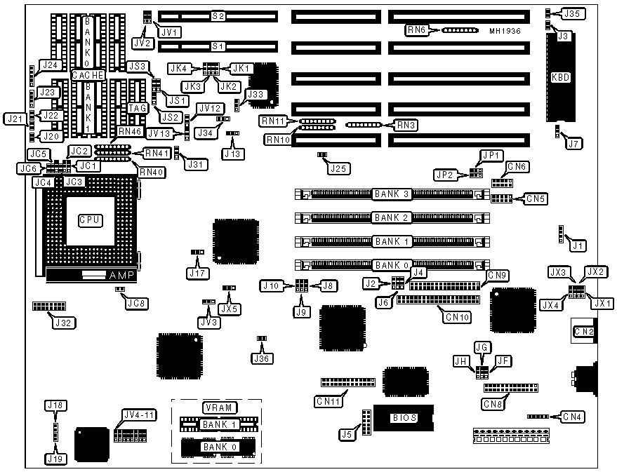
CONNECTIONS | |||
|
Purpose |
Location |
Purpose |
Location |
|
PS/2 mouse port (6-pin DIN) |
CN2 |
VGA connector |
J5 |
|
PS/2 mouse connector |
CN4 |
Turbo LED |
J20 |
|
Serial port 1 |
CN5 |
Turbo switch |
J21 |
|
Serial port 2 |
CN6 |
Reset switch |
J22 |
|
Parallel port |
CN8 |
Speaker |
J23 |
|
Floppy drive interface |
CN9 |
Power LED & keylock |
J24 |
|
IDE interface |
CN10 |
3.3V daughter board (80486DX4 only) |
J32 |
|
Video feature connector |
CN11 |
Green status LED |
J35 |
|
External battery |
J1 |
Hardware sleep |
J36 |
|
Green PC power |
J3 |
32-bit VESA Local bus slot |
S1 |
|
IDE interface LED |
J4 |
32-bit VESA Local bus slot |
S2 |
|
USER CONFIGURABLE SETTINGS | |||
|
Function |
Jumper |
Position | |
|
» |
IDE connector pin 27 open |
J2 |
Open |
|
IDE connector pin 27 linked to IOCHRDY signal |
J2 |
Closed | |
|
» |
IDE connector pin 28 open |
J6 |
Open |
|
IDE connector pin 28 linked to BALE signal |
J6 |
Closed | |
|
» |
CMOS memory normal operation |
J7 |
pins 1 & 2 closed |
|
CMOS memory clear |
J7 |
pins 2 & 3 closed | |
|
» |
Factory configured - do not alter |
J11 |
pins 1 & 2 closed |
|
» |
Factory configured - do not alter |
J25 |
N/A |
|
» |
80486DX4 clock mode 2.5x |
J31 |
pins 1 & 2 closed |
|
80486DX4 clock mode 2x |
J31 |
pins 2 & 3 closed | |
|
80486DX4 clock mode 3x |
J31 |
Open | |
|
» |
Factory configured - do not alter |
J33 |
pins 2 & 3 closed |
|
» |
Pentium Overdrive write-back |
JC8 |
pins 1 & 2 closed |
|
Pentium Overdrive write-through |
JC8 |
pins 2 & 3 closed | |
|
» |
Factory configured - do not alter |
JH |
pins 2 & 3 closed |
|
» |
Factory configured - do not alter |
JX6 |
pins 2 & 3 closed |
|
» |
Video upper physical address decode input select SA (26..31) |
JV5 |
pins 1 & 2 closed |
|
Video upper physical address decode input select SAUP (1..2) |
JV5 |
pins 2 & 3 closed | |
|
» |
Video DAC local access enabled |
JV6 |
pins 1 & 2 closed |
|
Video DAC local access disabled |
JV6 |
pins 2 & 3 closed | |
|
» |
Video memory address select 256KB |
JV11 |
pins 1 & 2 closed |
|
Video memory address select 64KB |
JV11 |
pins 2 & 3 closed | |
|
» |
Normal operation |
JV12 |
pins 1 & 2 closed |
|
Other IDE/VGA controller is installed at S1 |
JV12 |
pins 2 & 3 closed | |
|
» |
Normal operation |
JV13 |
pins 1 & 2 closed |
|
Other IDE/VGA controller is installed at S2 |
JV13 |
pins 2 & 3 closed | |
|
» |
CPU clock 1x |
JX1 |
pins 1 & 2 closed |
|
CPU clock 2x |
JX1 |
pins 2 & 3 closed | |
|
IDE CONFIGURATION | ||||
|
IDE |
Speed |
J8 |
J9 |
J10 |
|
Enabled |
0 |
pins 2 & 3 closed |
pins 2 & 3 closed |
pins 1 & 2 closed |
|
Enabled |
1 |
pins 2 & 3 closed |
pins 1 & 2 closed |
pins 1 & 2 closed |
|
Enabled |
2 |
pins 1 & 2 closed |
pins 1 & 2 closed |
pins 1 & 2 closed |
|
Disabled |
N/A |
N/A |
N/A |
pins 2 & 3 closed |
|
PARALLEL PORT CONFIGURATION | ||
|
Port |
JG |
JH |
|
Input |
pins 1 & 2 closed |
pins 1 & 2 closed |
|
Output |
pins 1 & 2 closed |
pins 2 & 3 closed |
|
Bi-directional |
pins 2 & 3 closed |
N/A |
|
VRAM CONFIGURATION | ||||
|
Video |
IRQ9 |
JV3 |
JV4 | |
| » |
Enabled |
Disabled |
pins 2 & 3 closed |
pins 1 & 2 closed |
|
Disabled |
Enabled |
pins 1 & 2 closed |
pins 2 & 3 closed | |
|
VRAM MEMORY CONFIGURATION | ||
|
Size |
Bank 0 |
Bank 1 |
|
1MB |
(2) 512K x 4 |
NONE |
|
2MB |
(2) 512K x 4 |
(2) 512K x 4 |
|
VIDEO MCLK SELECT | |||
|
MCLK |
J18 |
J19 | |
| » |
50MHz |
Open |
Open |
|
52MHz |
Open |
Closed | |
|
45MHz |
Closed |
Closed | |
|
38MHz |
Closed |
Open | |
|
MONITOR REFRESH RATE | |||
|
Rate |
JV7 |
JV8 | |
| » |
43Hz interlaced |
pins 2 & 3 closed |
pins 2 & 3 closed |
|
56Hz non-interlaced |
pins 2 & 3 closed |
pins 1 & 2 closed | |
|
60Hz non-interlaced |
pins 1 & 2 closed |
pins 2 & 3 closed | |
|
70/72Hz non-interlaced |
pins 1 & 2 closed |
pins 1 & 2 closed | |
|
VIDEO INTERLEAVE TIMING | |||
|
Select |
JV9 |
JV10 | |
| » |
1 NanoSeconds |
pins 1 & 2 closed |
pins 1 & 2 closed |
|
2 NanoSeconds |
pins 1 & 2 closed |
pins 2 & 3 closed | |
|
3 NanoSeconds |
pins 2 & 3 closed |
pins 1 & 2 closed | |
|
4 NanoSeconds |
pins 2 & 3 closed |
pins 2 & 3 closed | |
|
DRAM CONFIGURATION | ||||
|
Size |
Bank 0 |
Bank 1 |
Bank 2 |
Bank 3 |
|
1MB |
(1) 256K x 36 |
NONE |
NONE |
NONE |
|
1MB |
NONE |
(1) 256K x 36 |
NONE |
NONE |
|
1MB |
NONE |
NONE |
(1) 256K x 36 |
NONE |
|
2MB |
(1) 256K x 36 |
(1) 256K x 36 |
NONE |
NONE |
|
2MB |
(1) 256K x 36 |
NONE |
(1) 256K x 36 |
NONE |
|
2MB |
NONE |
NONE |
(1) 256K x 36 |
(1) 256K x 36 |
|
3MB |
(1) 256K x 36 |
(1) 256K x 36 |
(1) 256K x 36 |
NONE |
|
3MB |
NONE |
(1) 256K x 36 |
(1) 256K x 36 |
(1) 256K x 36 |
|
3MB |
(1) 256K x 36 |
NONE |
(1) 256K x 36 |
(1) 256K x 36 |
|
4MB |
(1) 256K x 36 |
(1) 256K x 36 |
(1) 256K x 36 |
(1) 256K x 36 |
|
4MB |
(1) 1M x 36 |
NONE |
NONE |
NONE |
|
4MB |
NONE |
(1) 1M x 36 |
NONE |
NONE |
|
4MB |
NONE |
NONE |
(1) 1M x 36 |
NONE |
|
5MB |
(1) 1M x 36 |
(1) 256K x 36 |
NONE |
NONE |
|
5MB |
(1) 256K x 36 |
(1) 1M x 36 |
NONE |
NONE |
|
5MB |
(1) 256K x 36 |
NONE |
(1) 1M x 36 |
NONE |
|
5MB |
(1) 1M x 36 |
NONE |
(1) 256K x 36 |
NONE |
|
5MB |
NONE |
(1) 256K x 36 |
(1) 4M x 36 |
NONE |
|
5MB |
NONE |
(1) 4M x 36 |
(1) 256K x 36 |
NONE |
|
6MB |
(1) 4M x 36 |
(1) 256K x 36 |
(1) 256K x 36 |
NONE |
|
6MB |
(1) 256K x 36 |
(1) 256K x 36 |
(1) 1M x 36 |
NONE |
|
6MB |
(1) 1M x 36 |
(1) 256K x 36 |
(1) 256K x 36 |
NONE |
|
6MB |
NONE |
(1) 1M x 36 |
(1) 256K x 36 |
(1) 256K x 36 |
|
6MB |
(1) 1M x 36 |
NONE |
(1) 256K x 36 |
(1) 256K x 36 |
|
7MB |
(1) 1M x 36 |
(1) 256K x 36 |
(1) 256K x 36 |
(1) 256K x 36 |
|
7MB |
(1) 256K x 36 |
(1) 1M x 36 |
(1) 256K x 36 |
(1) 256K x 36 |
|
8MB |
(1) 1M x 36 |
(1) 1M x 36 |
NONE |
NONE |
|
8MB |
(1) 1M x 36 |
NONE |
(1) 1M x 36 |
NONE |
|
8MB |
NONE |
NONE |
(1) 1M x 36 |
(1) 1M x 36 |
|
8MB |
NONE |
(1) 1M x 36 |
NONE |
(1) 1M x 36 |
|
9MB |
(1) 256K x 36 |
(1) 1M x 36 |
(1) 1M x 36 |
NONE |
|
9MB |
(1) 1M x 36 |
(1) 256K x 36 |
(1) 1M x 36 |
NONE |
|
9MB |
(1) 1M x 36 |
(1) 1M x 36 |
(1) 256K x 36 |
NONE |
|
9MB |
NONE |
(1) 256K x 36 |
(1) 1M x 36 |
(1) 1M x 36 |
|
9MB |
(1) 256K x 36 |
NONE |
(1) 1M x 36 |
(1) 1M x 36 |
|
10MB |
(1) 256K x 36 |
(1) 256K x 36 |
(1) 1M x 36 |
(1) 1M x 36 |
|
10MB |
(1) 1M x 36 |
(1) 1M x 36 |
(1) 256K x 36 |
(1) 256K x 36 |
|
12MB |
(1) 1M x 36 |
(1) 1M x 36 |
(1) 1M x 36 |
NONE |
|
12MB |
NONE |
(1) 1M x 36 |
(1) 1M x 36 |
(1) 1M x 36 |
|
DRAM CONFIGURATION (CONTINUED) | ||||
|
Size |
Bank 0 |
Bank 1 |
Bank 2 |
Bank 3 |
|
12MB |
(1) 1M x 36 |
NONE |
(1) 1M x 36 |
(1) 1M x 36 |
|
13MB |
(1) 256K x 36 |
(1) 1M x 36 |
(1) 1M x 36 |
(1) 1M x 36 |
|
13MB |
(1) 1M x 36 |
(1) 256K x 36 |
(1) 1M x 36 |
(1) 1M x 36 |
|
16MB |
(1) 1M x 36 |
(1) 1M x 36 |
(1) 1M x 36 |
(1) 1M x 36 |
|
16MB |
(1) 4M x 36 |
NONE |
NONE |
NONE |
|
16MB |
NONE |
(1) 4M x 36 |
NONE |
NONE |
|
16MB |
NONE |
NONE |
(1) 4M x 36 |
NONE |
|
17MB |
(1) 4M x 36 |
(1) 256K x 36 |
NONE |
NONE |
|
17MB |
(1) 256K x 36 |
(1) 4M x 36 |
NONE |
NONE |
|
17MB |
(1) 256K x 36 |
NONE |
(1) 4M x 36 |
NONE |
|
17MB |
NONE |
(1) 4M x 36 |
(1) 256K x 36 |
NONE |
|
17MB |
NONE |
(1) 256K x 36 |
(1) 4M x 36 |
NONE |
|
18MB |
(1) 4M x 36 |
(1) 256K x 36 |
(1) 256K x 36 |
NONE |
|
18MB |
(1) 256K x 36 |
(1) 256K x 36 |
(1) 4M x 36 |
NONE |
|
18MB |
(1) 256K x 36 |
(1) 4M x 36 |
(1) 256K x 36 |
NONE |
|
18MB |
NONE |
(1) 4M x 36 |
(1) 256K x 36 |
(1) 256K x 36 |
|
19MB |
(1) 4M x 36 |
(1) 256K x 36 |
(1) 256K x 36 |
(1) 256K x 36 |
|
19MB |
(1) 256K x 36 |
(1) 4M x 36 |
(1) 256K x 36 |
(1) 256K x 36 |
|
20MB |
(1) 4M x 36 |
(1) 1M x 36 |
NONE |
NONE |
|
20MB |
(1) 1M x 36 |
(1) 4M x 36 |
NONE |
NONE |
|
20MB |
(1) 1M x 36 |
NONE |
(1) 4M x 36 |
NONE |
|
20MB |
NONE |
(1) 1M x 36 |
(1) 4M x 36 |
NONE |
|
20MB |
NONE |
(1) 4M x 36 |
(1) 1M x 36 |
NONE |
|
21MB |
(1) 4M x 36 |
(1) 1M x 36 |
(1) 256K x 36 |
NONE |
|
21MB |
(1) 256K x 36 |
(1) 1M x 36 |
(1) 4M x 36 |
NONE |
|
21MB |
(1) 256K x 36 |
(1) 4M x 36 |
(1) 1M x 36 |
NONE |
|
21MB |
(1) 1M x 36 |
(1) 256K x 36 |
(1) 4M x 36 |
NONE |
|
21MB |
(1) 1M x 36 |
(1) 4M x 36 |
(1) 256K x 36 |
NONE |
|
22MB |
(1) 4M x 36 |
(1) 1M x 36 |
(1) 256K x 36 |
(1) 256K x 36 |
|
22MB |
(1) 1M x 36 |
(1) 4M x 36 |
(1) 256K x 36 |
(1) 256K x 36 |
|
24MB |
(1) 4M x 36 |
(1) 1M x 36 |
(1) 1M x 36 |
NONE |
|
24MB |
(1) 1M x 36 |
(1) 1M x 36 |
(1) 4M x 36 |
NONE |
|
24MB |
(1) 1M x 36 |
(1) 4M x 36 |
(1) 1M x 36 |
NONE |
|
24MB |
NONE |
(1) 4M x 36 |
(1) 1M x 36 |
(1) 1M x 36 |
|
25MB |
(1) 256K x 36 |
(1) 4M x 36 |
(1) 1M x 36 |
(1) 1M x 36 |
|
28MB |
(1) 4M x 36 |
(1) 1M x 36 |
(1) 1M x 36 |
(1) 1M x 36 |
|
28MB |
(1) 1M x 36 |
(1) 4M x 36 |
(1) 1M x 36 |
(1) 1M x 36 |
|
32MB |
(1) 4M x 36 |
(1) 4M x 36 |
NONE |
NONE |
|
32MB |
NONE |
(1) 4M x 36 |
(1) 4M x 36 |
NONE |
|
32MB |
NONE |
NONE |
(1) 4M x 36 |
(1) 4M x 36 |
|
33MB |
(1) 4M x 36 |
(1) 4M x 36 |
(1) 256K x 36 |
NONE |
|
DRAM CONFIGURATION (CONTINUED) | ||||
|
Size |
Bank 0 |
Bank 1 |
Bank 2 |
Bank 3 |
|
33MB |
(1) 256K x 36 |
(1) 4M x 36 |
(1) 4M x 36 |
NONE |
|
33MB |
NONE |
(1) 256K x 36 |
(1) 4M x 36 |
(1) 4M x 36 |
|
33MB |
(1) 256K x 36 |
NONE |
(1) 4M x 36 |
(1) 4M x 36 |
|
34MB |
(1) 4M x 36 |
(1) 4M x 36 |
(1) 256K x 36 |
(1) 256K x 36 |
|
34MB |
(1) 256K x 36 |
(1) 256K x 36 |
(1) 4M x 36 |
(1) 4M x 36 |
|
36MB |
(1) 4M x 36 |
(1) 4M x 36 |
(1) 1M x 36 |
NONE |
|
36MB |
(1) 1M x 36 |
(1) 4M x 36 |
(1) 4M x 36 |
NONE |
|
36MB |
NONE |
(1) 1M x 36 |
(1) 4M x 36 |
(1) 4M x 36 |
|
36MB |
(1) 1M x 36 |
NONE |
(1) 4M x 36 |
(1) 4M x 36 |
|
37MB |
(1) 256K x 36 |
(1) 1M x 36 |
(1) 4M x 36 |
(1) 4M x 36 |
|
37MB |
(1) 1M x 36 |
(1) 256K x 36 |
(1) 4M x 36 |
(1) 4M x 36 |
|
40MB |
(1) 4M x 36 |
(1) 4M x 36 |
(1) 1M x 36 |
(1) 1M x 36 |
|
40MB |
(1) 1M x 36 |
(1) 1M x 36 |
(1) 4M x 36 |
(1) 4M x 36 |
|
48MB |
(1) 4M x 36 |
(1) 4M x 36 |
(1) 4M x 36 |
NONE |
|
48MB |
NONE |
(1) 4M x 36 |
(1) 4M x 36 |
(1) 4M x 36 |
|
49MB |
(1) 256K x 36 |
(1) 4M x 36 |
(1) 4M x 36 |
(1) 4M x 36 |
|
52MB |
(1) 1M x 36 |
(1) 4M x 36 |
(1) 4M x 36 |
(1) 4M x 36 |
|
64MB |
(1) 4M x 36 |
(1) 4M x 36 |
(1) 4M x 36 |
(1) 4M x 36 |
|
64MB |
(1) 8M x 36 |
NONE |
(1) 8M x 36 |
NONE |
|
CACHE CONFIGURATION | |||
|
Size |
Bank 0 |
Bank 1 |
TAG |
|
64KB |
(4) 8K x 8 |
(4) 8K x 8 |
(1) 8K x 8 |
|
128KB |
NONE |
(4) 32K x 8 |
(1) 8K x 8 |
|
256KB |
(4) 32K x 8 |
(4) 32K x 8 |
(1) 32K x 8 |
|
CACHE JUMPER CONFIGURATION | |||
|
Size |
JS1 |
JS2 |
JS3 |
|
64KB |
pins 1 & 2 closed |
pins 1 & 2 closed |
pins 1 & 2 closed |
|
128KB |
pins 1 & 2 closed |
pins 2 & 3 closed |
pins 2 & 3 closed |
|
256KB |
pins 2 & 3 closed |
pins 2 & 3 closed |
pins 1 & 2 closed |
|
CPU SPEED CONFIGURATION | ||||
|
Speed |
JK1 |
JK2 |
JK3 |
JK4 |
|
25MHz |
pins 2 & 3 closed |
pins 1 & 2 closed |
pins 2 & 3 closed |
pins 1 & 2 closed |
|
33MHz |
pins 2 & 3 closed |
pins 2 & 3 closed |
pins 1 & 2 closed |
pins 1 & 2 closed |
|
40MHz |
pins 1 & 2 closed |
pins 1 & 2 closed |
pins 2 & 3 closed |
pins 1 & 2 closed |
|
50iMHz |
pins 2 & 3 closed |
pins 1 & 2 closed |
pins 2 & 3 closed |
pins 1 & 2 closed |
|
50MHz |
pins 2 & 3 closed |
pins 1 & 2 closed |
pins 2 & 3 closed |
pins 2 & 3 closed |
|
66iMHz |
pins 2 & 3 closed |
pins 2 & 3 closed |
pins 1 & 2 closed |
pins 1 & 2 closed |
|
CPU TYPE CONFIGURATION | |||||
|
Type |
JC1 |
JC2 |
JC3 |
JC4 |
JC6 |
|
80486SX |
pins 2 & 3 |
pins 2 & 3 |
Open |
pins 1 & 2 |
Open |
|
CX486S |
pins 2 & 3 |
pins 2 & 3 |
Open |
pins 1 & 2 |
Closed |
|
CX486S+ |
pins 1 & 2 |
pins 1 & 2 |
Open |
pins 1 & 2 |
Open |
|
CX487S |
pins 1 & 2 |
pins 1 & 2 |
Open |
pins 1 & 2 |
Open |
|
AM486DXL |
pins 1 & 2 |
pins 1 & 2 |
Open |
pins 1 & 2 |
Closed |
|
CX486DX |
pins 1 & 2 |
pins 1 & 2 |
Open |
pins 1 & 2 |
Open |
|
80486DX |
pins 1 & 2 |
pins 1 & 2 |
Open |
pins 1 & 2 |
Closed |
|
80486DX2 |
pins 1 & 2 |
pins 1 & 2 |
Open |
pins 1 & 2 |
Closed |
|
80486DX4 |
pins 1 & 2 |
pins 1 & 2 |
Open |
pins 1 & 2 |
Closed |
|
Pentium Overdrive |
pins 1 & 2 |
pins 1 & 2 |
Closed |
pins 2 & 3 |
Closed |
|
Note:Pins designated should be in the closed position. | |||||
|
CPU TYPE CONFIGURATION (CONTINUED) | ||||
|
Type |
JC5 |
RN40 |
RN41 |
RN46 |
|
80486SX |
Open |
Not installed |
Not installed |
Not installed |
|
CX486S |
Open |
Installed |
Not installed |
Not installed |
|
CX486S+ |
Open |
Installed |
Not installed |
Not installed |
|
CX487S |
Open |
Installed |
Not installed |
Not installed |
|
AM486DXL |
Open |
Not installed |
Not installed |
Installed |
|
CX486DX |
Open |
Installed |
Not installed |
Not installed |
|
80486DX |
Open |
Not installed |
Not installed |
Not installed |
|
80486DX2 |
Open |
Not installed |
Not installed |
Not installed |
|
80486DX4 |
Closed |
Not installed |
Installed |
Not installed |
|
Pentium Overdrive |
Closed |
Not installed |
Not installed |
Not installed |
|
CPU TYPE CONFIGURATION (MANUFACTURER) | ||
|
Type |
J17 |
J34 |
|
Intel |
pins 1 & 2 closed |
pins 1 & 2 closed |
|
Cyrix |
pins 2 & 3 closed |
pins 2 & 3 closed |
|
CPU TYPE IRQ SELECTION | |||
|
Select |
J13 |
JX2 |
JX5 |
|
IRQ15 |
pins 2 & 3 closed |
pins 1 & 2 closed |
pins 1 & 2 closed |
|
SMI |
pins 1 & 2 closed |
pins 2 & 3 closed |
pins 2 & 3 closed |
|
Note:Jumper pins 1 & 2 of J13 if JX2 and JX5 are set at SMI and you wish to use the IRQ15 function. | |||
|
KEYBOARD CONFIGURATION | ||||||
|
Select |
JX3 |
JX4 |
RN3 |
RN6 |
RN10 |
RN11 |
|
External |
pins 1 & 2 |
pins 1 & 2 |
Not installed |
Installed |
Not installed |
Installed |
|
Internal |
pins 2 & 3 |
pins 2 & 3 |
Installed |
Not installed |
Installed |
Not installed |
|
Note:Pins designated should be in the closed position. | ||||||
|
VESA WAIT STATE/BUS SPEED CONFIGURATION | |||
|
CPU speed |
Wait states |
JV1 |
JV2 |
|
< 33MHz |
0 wait states |
pins 2 & 3 closed |
pins 2 & 3 closed |
|
> 33MHz |
1 wait state |
pins 1 & 2 closed |
pins 1 & 2 closed |
|
PC87332 ECP DMA CHANNEL SELECT | |||
|
DREQ |
DACK |
JP1 |
JP2 |
|
1 |
1 |
pins 2 & 3 closed |
pins 2 & 3 closed |
|
3 |
3 |
pins 1 & 2 closed |
pins 1 & 2 closed |
|
NSS87311/312 BASE I/O ADDRESS SELECT | ||
|
Index Address |
Data Address |
JF |
|
26Eh |
26Fh |
pins 1 & 2 closed |
|
398h |
399h |
pins 2 & 3 closed |
|
NSS87332 BASE I/O ADDRESS SELECT | |||
|
Index Address |
Data Address |
JF |
JG |
|
2Eh |
2Fh |
pins 1 & 2 closed |
pins 1 & 2 closed |
|
26Eh |
26Fh |
pins 1 & 2 closed |
pins 2 & 3 closed |
|
15Ch |
15Dh |
pins 2 & 3 closed |
pins 1 & 2 closed |
|
398h |
399h |
pins 2 & 3 closed |
pins 2 & 3 closed |