ICL
INDIANA C-SERIES/S-SERIES
|
Processor |
80486SX/80486SX2/80486DX/80486DX2/AM486DX4/80486DX4 |
|
Processor Speed |
25/33/50(internal)/66(internal)/75(internal)/100(internal)MHz |
|
Chip Set |
Acer |
|
Max. Onboard DRAM |
36MB |
|
Cache |
128/256KB |
|
BIOS |
Acer |
|
Dimensions |
295mm x 254mm |
|
I/O Options |
PS/2 mouse port, parallel port, serial ports (2), VGA port, VGA feature connector, floppy drive interface, IDE interface |
|
NPU Options |
None |
|
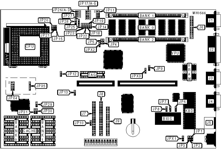
CONNECTIONS | |||
|
Purpose |
Location |
Purpose |
Location |
|
VGA port |
J1 |
VGA feature connector |
J6 |
|
Parallel port |
J2 |
IDE interface 1 |
J7 |
|
Serial port 1 |
J3 |
IDE interface 2 |
J8 |
|
Serial port 2 |
J4 |
Floppy drive interface |
J9 |
|
PS/2 mouse port |
J5 |
DX4 voltage kit connectors |
JPX4 & JPX5 |
|
USER CONFIGURABLE SETTINGS | |||
|
Function |
Jumper |
Position | |
|
» |
Normal BIOS startup display |
JP1 |
pins 1 & 2 closed |
|
BIOS displays Acer logo |
JP1 |
pins 2 & 3 closed | |
|
» |
Password enabled |
JP2 |
pins 1 & 2 closed |
|
Password disabled |
JP2 |
pins 2 & 3 closed | |
|
» |
Boot mode select normal boot |
JP3 |
pins 1 & 2 closed |
|
Boot mode select mono/COM1 boot |
JP3 |
pins 2 & 3 closed | |
|
» |
First 8MB of memory enabled |
JP4 |
pins 1 & 2 closed |
|
First 8MB of memory disabled |
JP4 |
pins 2 & 3 closed | |
|
» |
On-board memory enabled |
JP5 |
pins 2 & 3 closed |
|
On-board memory disabled |
JP5 |
pins 1 & 2 closed | |
|
» |
Super I/O chip enabled |
JP6 |
pins 2 & 3 closed |
|
Super I/O chip disabled |
JP6 |
pins 1 & 2 closed | |
|
» |
VGA port enabled |
JP9 |
pins 2 & 3 closed |
|
VGA port disabled |
JP9 |
pins 1 & 2 closed | |
|
» |
IDE address port select 0F4h, 0F8h, and 0FCh |
JP10 |
pins 1 & 2 closed |
|
IDE address port select 074h, 078h, and 07Ch |
JP10 |
pins 2 & 3 closed | |
|
» |
Reset button mode normal |
JP28 |
pins 2 & 3 closed |
|
Reset button mode suspend/resume |
JP28 |
pins 1 & 2 closed | |
|
» |
IDE interface enabled |
JP29 |
pins 2 & 3 closed |
|
IDE interface disabled |
JP29 |
pins 1 & 2 closed | |
|
» |
BIOS type select EPROM |
JPX1 |
pins 2 & 3 closed |
|
BIOS type select flash |
JPX1 |
pins 1 & 2 closed | |
|
» |
Factory configured - do not alter |
JPX3 |
N/A |
|
DRAM CONFIGURATION | |||
|
Size |
Bank 0 |
Bank 1 |
Bank 2 |
|
4MB |
(8) 441000 |
NONE |
NONE |
|
8MB |
(8) 441000 |
(1) 1M x 36 |
NONE |
|
12MB |
(8) 441000 |
(1) 1M x 36 |
(1) 1M x 36 |
|
20MB |
(8) 441000 |
(1) 4M x 36 |
NONE |
|
24MB |
(8) 441000 |
(1) 4M x 36 |
(1) 1M x 36 |
|
36MB |
(8) 441000 |
(1) 4M x 36 |
(1) 4M x 36 |
|
CACHE CONFIGURATION | |||
|
Size |
Bank 0 |
Bank 1 |
TAG |
|
128KB |
(4) 32K x 8 |
NONE |
(1) 32K x 8 |
|
256KB |
(4) 32K x 8 |
(4) 32K x 8 |
(1) 32K x 8 |
|
CACHE JUMPER CONFIGURATION | ||
|
Size |
JP30 |
JP31 |
|
128KB |
pins 1 & 2 closed |
pins 1 & 2 closed |
|
256KB |
pins 2 & 3 closed |
pins 2 & 3 closed |
|
CPU TYPE CONFIGURATION | |||||
|
Type |
JPX2 |
JP13 |
JP14 |
JP15 |
JP17 |
|
80486SX |
2 & 3 |
2 & 3 |
2 & 3 |
2 & 3 |
2 & 3 |
|
80486SX2 |
2 & 3 |
2 & 3 |
2 & 3 |
2 & 3 |
2 & 3 |
|
80486DX |
2 & 3 |
2 & 3 |
2 & 3 |
2 & 3 |
2 & 3 |
|
80486DX2 |
2 & 3 |
2 & 3 |
2 & 3 |
2 & 3 |
2 & 3 |
|
AM486DX4 |
2 & 3 |
2 & 3 |
2 & 3 |
2 & 3 |
2 & 3 |
|
80486DX4 |
2 & 3 |
2 & 3 |
2 & 3 |
2 & 3 |
2 & 3 |
|
Note: Pins designated should be in the closed position. | |||||
|
CPU TYPE CONFIGURATION (CON’T) | |||||
|
Type |
JP18 |
JP19 |
JP20 |
JP21 |
JP22 |
|
80486SX |
2 & 3 |
2 & 3 |
2 & 3 |
2 & 3 |
2 & 3 |
|
80486SX2 |
2 & 3 |
2 & 3 |
2 & 3 |
2 & 3 |
2 & 3 |
|
80486DX |
2 & 3 |
1 & 2 |
2 & 3 |
2 & 3 |
1 & 2 |
|
80486DX2 |
2 & 3 |
1 & 2 |
2 & 3 |
2 & 3 |
1 & 2 |
|
AM486DX4 |
1 & 2 |
1 & 2 |
2 & 3 |
2 & 3 |
2 & 3 |
|
80486DX4 |
1 & 2 |
1 & 2 |
2 & 3 |
2 & 3 |
2 & 3 |
|
Note: Pins designated should be in the closed position. | |||||
|
CPU TYPE CONFIGURATION | |||||
|
Type |
JP23 |
JP25 |
JP26 |
JP27 |
JP32 |
|
80486SX |
2 & 3 |
2 & 3 |
2 & 3 |
3 & 4 |
1 & 2 |
|
80486SX2 |
2 & 3 |
2 & 3 |
2 & 3 |
3 & 4 |
1 & 2 |
|
80486DX |
2 & 3 |
2 & 3 |
1 & 2 |
3 & 4 |
1 & 2 |
|
80486DX2 |
2 & 3 |
2 & 3 |
1 & 2 |
3 & 4 |
1 & 2 |
|
AM486DX4 |
2 & 3 |
2 & 3 |
2 & 3 |
3 & 4 |
1 & 2 |
|
80486DX4 |
2 & 3 |
2 & 3 |
2 & 3 |
3 & 4 |
1 & 2 |
|
Note: Pins designated should be in the closed position. The locations of JP27 & JP32 are unidentified. | |||||
|
CPU SPEED CONFIGURATION | ||
|
Speed |
JP11 |
JP12 |
|
25MHz |
pins 1 & 5 closed |
pins 2 & 3 closed |
|
33MHz |
pins 2 & 6 closed |
pins 2 & 3 closed |
|
50iMHz |
pins 1 & 5 closed |
pins 2 & 3 closed |
|
66iMHz |
pins 2 & 6 closed |
pins 2 & 3 closed |
|
75iMHz |
pins 1 & 5 closed |
pins 2 & 3 closed |
|
100iMHz |
pins 2 & 6 closed |
pins 2 & 3 closed |
|
CPU SPEED CONFIGURATION (80486DX4 ONLY) | |
|
Speed |
JP27 |
|
2x |
pins 2 & 3 closed |
|
2.5x |
pins 1 & 2 closed |
|
3x |
pins 3 & 4 closed |
|
CPU VOLTAGE CONFIGURATION (80486DX4-100 ONLY) | |
|
Voltage |
JMP1 |
|
3.45v |
pins 1 & 5 closed |
|
3.6v |
pins 2 & 6 closed |
|
3.8v |
pins 3 & 7 closed |
|
4v |
pins 4 & 8 closed |
|
Note: JMP1 is located on the voltage regulator. | |
|
PARALLEL PORT DMA CHANNEL CONFIGURATION | ||||
|
» DRQ |
DACK |
JP7 |
JP8 | |
| » |
3 |
3 |
pins 1 & 2 closed |
pins 1 & 2 closed |
| » |
3 |
1 |
pins 1 & 2 closed |
pins 2 & 3 closed |
| » |
1 |
3 |
pins 2 & 3 closed |
pins 1 & 2 closed |
| » |
1 |
1 |
pins 2 & 3 closed |
pins 2 & 3 closed |