INFORMTECH INTERNATIONAL, INC.
IT486SMVG MINI VER. 1.1
|
Processor |
80486SX/80487SX/80486DX/80486DX2/Pentium Overdrive |
|
Processor Speed |
20/25/33/40(internal)50/50(internal)/66(internal)MHz |
|
Chip Set |
FOREX |
|
Max. Onboard DRAM |
64MB |
|
Cache |
64/128/256KB |
|
BIOS |
AMI |
|
Dimensions |
230mm x 218mm |
|
I/O Options |
32-bit VESA local bus slots (3) |
|
NPU Options |
None |
|
CONNECTIONS |
|||
|
Purpose |
Location |
Purpose |
Location |
|
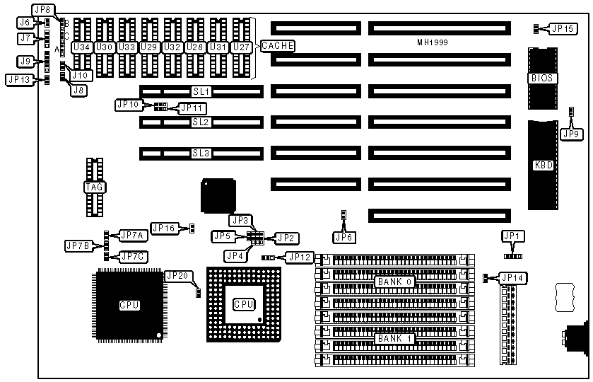
Turbo LED |
J6 |
Reset switch |
J10 |
|
Speaker |
J7 |
External battery |
JP1 |
|
Turbo switch |
J8 |
32-bit VESA Local bus slots |
SL1 |
|
Power LED & keylock |
J9 |
32-bit VESA Local bus slots |
SL2 & SL3 |
|
USER CONFIGURABLE SETTINGS |
|||
|
Function |
Jumper |
Position |
|
|
» |
CPU type select - 486DX/DX2/P24T (PGA) |
JP2 |
pins 1 & 2 closed |
|
|
CPU type select - 486SX/DX (PQFP) & 487SX/P23T (PGA) |
JP2 |
pins 2 & 3 closed |
|
» |
CPU type select -PGA |
JP3 & JP4 |
pins 1 & 2 closed |
|
|
CPU type select -PQFP |
JP3 & JP4 |
pins 2 & 3 closed |
|
» |
PFPQ disabled |
JP5 |
Closed |
|
|
PFPQ enabled |
JP5 |
Open |
|
» |
CMOS memory normal operation |
JP6 |
Open |
|
|
CMOS memory clear |
JP6 |
Closed |
|
» |
Factory configured - do not alter |
JP9 |
Open |
|
» |
CPU type select - 486CPU |
JP12 |
pins 1 & 2 closed |
|
|
CPU type select - P24T CPU |
JP12 |
pins 2 & 3 closed |
|
» |
Factory configured - do not alter |
JP13 |
Open |
|
» |
Factory configured - do not alter |
JP14 |
Open |
|
» |
Factory configured - do not alter |
JP15 |
Open |
|
» |
Factory configured - do not alter |
JP16 |
Open |
|
» |
Cyrix CPU type select - CX486DX |
JP20 |
Open |
|
|
Cyrix CPU type select - CX486DX2 |
JP20 |
Closed |
|
DRAM CONFIGURATION |
||
|
Size |
Bank 0 |
Bank 1 |
|
1MB |
(4) 256K x 9 |
NONE |
|
2MB |
(4) 256K x 9 |
(4) 256K x 9 |
|
4MB |
(4) 1M x 9 |
NONE |
|
5MB |
(4) 256K x 9 |
(4) 1M x 9 |
|
8MB |
(4) 1M x 9 |
(4) 1M x 9 |
|
16MB |
(4) 4M x 9 |
NONE |
|
20MB |
(4) 1M x 9 |
(4) 4M x 9 |
|
32MB |
(4) 4M x 9 |
(4) 4M x 9 |
|
64MB |
(4) 16M x 9 |
NONE |
|
CACHE CONFIGURATION |
|||
|
Size |
Bank 0 |
Bank 1 |
TAG |
|
64KB |
(4) 8K x 8 |
(4) 8K x 8 |
(1) 8K x 8 |
|
128KB |
(4) 32K x 8 |
NONE |
(1) 8K x 8 |
|
256KB |
(4) 32K x 8 |
(4) 32K x 8 |
(1) 32K x 8 |
|
Note: Bank 0 = U31, U32, U33, U34 Bank 1 = U27, U28, U29, U30 |
|||
|
CACHE JUMPER CONFIGURATION |
|||
|
Size |
JP8A |
JP8B |
JP8C |
|
64KB |
pins 2 & 3 closed |
pins 1 & 2 closed |
pins 2 & 3 closed |
|
128KB |
pins 1 & 2 closed |
pins 2 & 3 closed |
pins 1 & 2 closed |
|
256KB |
pins 1 & 2 closed |
pins 1 & 2 closed |
pins 1 & 2 closed |
|
CLOCK SPEED CONFIGURATION |
|||
|
Speed |
JP7A |
JP7B |
JP7C |
|
20MHz |
Open |
Closed |
Closed |
|
25MHz |
Closed |
Open |
Open |
|
33MHz |
Open |
Open |
Open |
|
40MHz |
Closed |
Closed |
Open |
|
50MHz |
Open |
Closed |
Open |
|
50iMHz |
Closed |
Open |
Open |
|
66iMHz |
Open |
Open |
Open |
|
VESA WAIT STATE/BUS SPEED CONFIGURATION |
|||
|
CPU speed |
Wait states |
JP10 |
JP11 |
|
< 33MHz |
0 wait states |
pins 1 & 2 closed |
pins 1 & 2 closed |
|
> 33MHz |
1 wait state |
pins 2 & 3 closed |
pins 2 & 3 closed |