INTEL CORPORATION
CLASSIC R
|
Processor |
80486SX/80486DX/80486DX2 |
|
Processor Speed |
25/33/50(internal)/66(internal)MHz |
|
Chip Set |
VLSI |
|
Max. Onboard DRAM |
32MB |
|
Cache |
64/128/256KB |
|
BIOS |
Phoenix |
|
Dimensions |
330mm x 218mm |
|
I/O Options |
Floppy drive interface, IDE interface, parallel port, PS/2 mouse port, serial ports (2), VESA feature connector, VGA port, riser slot |
|
NPU Options |
None |
|
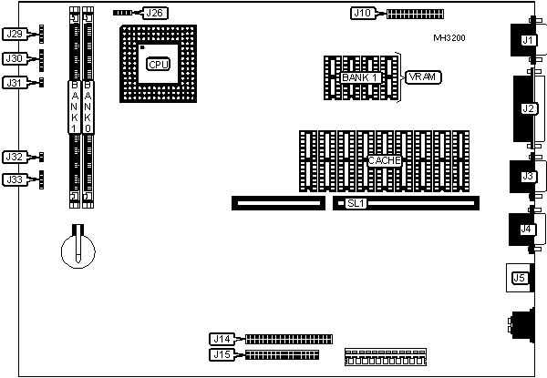
CONNECTIONS | |||
|
Purpose |
Location |
Purpose |
Location |
|
VGA port |
J1 |
Chassis fan power |
J26 |
|
Parallel port |
J2 |
IDE interface LED |
J29 |
|
Serial port 2 |
J3 |
Power LED & keylock |
J30 |
|
Serial port 1 |
J4 |
Reset switch |
J31 |
|
PS/2 mouse port |
J5 |
Chassis fan power |
J32 |
|
VESA feature connector |
J10 |
Speaker |
J33 |
|
IDE interface |
J14 |
Riser slot |
SL1 |
|
Floppy drive interface |
J15 | ||
|
USER CONFIGURABLE SETTINGS | |||
|
Function |
Jumper |
Position | |
|
» |
12v to flash BIOS enabled |
J12 |
pins 1 & 2 closed |
|
12v to flash BIOS disabled |
J12 |
pins 2 & 3 closed | |
|
» |
Flash BIOS recovery mode disabled |
J13 |
pins 1 & 2 closed |
|
Flash BIOS recovery mode enabled |
J13 |
pins 2 & 3 closed | |
|
» |
On board video enabled |
J16 |
pins 1 & 2 closed |
|
On board video disabled |
J16 |
pins 2 & 3 closed | |
|
» |
Floppy drive write protect enabled |
J17 |
pins 2 & 3 closed |
|
Floppy drive write protect disabled |
J17 |
pins 1 & 2 closed | |
|
» |
Password enabled |
J20 |
pins 2 & 3 closed |
|
Password clear |
J20 |
pins 1 & 2 closed | |
|
» |
CMOS access enabled |
J21 |
pins 1 & 2 closed |
|
CMOS access disabled |
J21 |
pins 2 & 3 closed | |
|
» |
CMOS memory normal operation |
J28 |
Closed |
|
CMOS memory clear |
J28 |
Open | |
|
Note: The location of the above jumpers are unidentified. | |||
|
DRAM CONFIGURATION | ||
|
Size |
Bank 0 |
Bank 1 |
|
2MB |
(1) 512K x 36 |
NONE |
|
4MB |
(1) 512K x 36 |
(1) 512K x 36 |
|
4MB |
(1) 1M x 36 |
NONE |
|
6MB |
(1) 512K x 36 |
(1) 1M x 36 |
|
6MB |
(1) 1M x 36 |
(1) 512K x 36 |
|
8MB |
(1) 1M x 36 |
(1) 1M x 36 |
|
8MB |
(1) 2M x 36 |
NONE |
|
10MB |
(1) 512K x 36 |
(1) 2M x 36 |
|
10MB |
(1) 2M x 36 |
(1) 512K x 36 |
|
12MB |
(1) 1M x 36 |
(1) 2M x 36 |
|
12MB |
(1) 2M x 36 |
(1) 1M x 36 |
|
16MB |
(1) 2M x 36 |
(1) 2M x 36 |
|
16MB |
(1) 4M x 36 |
NONE |
|
18MB |
(1) 512K x 36 |
(1) 4M x 36 |
|
18MB |
(1) 4M x 36 |
(1) 512K x 36 |
|
20MB |
(1) 1M x 36 |
(1) 4M x 36 |
|
20MB |
(1) 4M x 36 |
(1) 1M x 36 |
|
24MB |
(1) 2M x 36 |
(1) 4M x 36 |
|
24MB |
(1) 4M x 36 |
(1) 2M x 36 |
|
32MB |
(1) 4M x 36 |
(1) 4M x 36 |
|
CACHE CONFIGURATION | |||
|
Size |
Bank 0 |
Bank 1 |
TAG |
|
64KB |
(4) 8K x 8 |
(4) 8K x 8 |
(1) 8K x 8 |
|
128KB |
(4) 32K x 8 |
NONE |
(1) 8K x 8 |
|
256KB |
(4) 32K x 8 |
(4) 32K x 8 |
(1) 32K x 8 |
|
Note: The orientation of Banks 0 & 1 and TAG is unidentified. | |||
|
CACHE JUMPER CONFIGURATION | ||||
|
Size |
J11 pins 1 & 2 |
J11 pins 3 & 4 |
J11 pins 5 & 6 |
J11 pins 7 & 8 |
|
64KB |
Open |
Open |
Open |
Open |
|
128KB |
Closed |
Open |
Closed |
Open |
|
256KB |
Closed |
Closed |
Open |
Closed |
|
Note: The location of J11 is unidentified. | ||||
|
CPU TYPE CONFIGURATION | ||||
|
Type |
J22 |
J23 |
j24 |
j25 |
|
80486SX (PQFP) |
pins 2 & 3 closed |
pins 1 & 2 closed |
pins 1 & 2 closed |
pins 1 & 2 closed |
|
80486SX (PGA) |
pins 1 & 2 closed |
pins 2 & 3 closed |
pins 2 & 3 closed |
pins 2 & 3 closed |
|
80486DX |
pins 2 & 3 closed |
pins 1 & 2 closed |
pins 1 & 2 closed |
pins 1 & 2 closed |
|
80486DX2 |
pins 2 & 3 closed |
pins 1 & 2 closed |
pins 1 & 2 closed |
pins 1 & 2 closed |
|
Note: The locations of J22, J23, J24 & J25 are unidentified. The location of the PQFP socket is unidentified. | ||||
|
CPU SPEED CONFIGURATION | ||
|
Speed |
J18 |
J19 |
|
25MHz |
pins 1 & 2 closed |
pins 1 & 2 closed |
|
33MHz |
pins 1 & 2 closed |
pins 2 & 3 closed |
|
50iMHz |
pins 1 & 2 closed |
pins 1 & 2 closed |
|
66iMHz |
pins 1 & 2 closed |
pins 2 & 3 closed |
|
Note: The locations of J18 & J19 are unidentified. | ||
|
VRAM CONFIGURATION | ||
|
Size |
Bank 0 |
Bank 1 |
|
512KB |
512KB |
NONE |
|
1MB |
512KB |
(4) 256K x 4 |
|
Note: Bank 0 is factory installed and is not configurable. The location is unidentified. | ||