INTEL CORPORATION
ADVANCED/RH LPX
|
Processor |
Pentium |
|
Processor Speed |
75/90/100/120/133/150/166MHz |
|
Chip Set |
Intel |
|
Video Chip Set |
ATI |
|
Maximum Onboard Memory |
512MB (EDO supported) |
|
Maximum Video Memory |
4MB |
|
Cache |
256/512KB |
|
BIOS |
Intel |
|
Dimensions |
330mm x 228mm |
|
I/O Options |
CD-ROM interface, floppy drive interface, green PC connector, IDE interfaces (2), parallel port, PS/2 mouse port, serial ports (2), VGA port, riser slot, cache slot, IR connector, USB connector, telephony connector, wavetable connector, audio out connector, microphone in connector, MIDI/audio connector, ATI media connector, power supply remote connector |
|
NPU Options |
None |
|
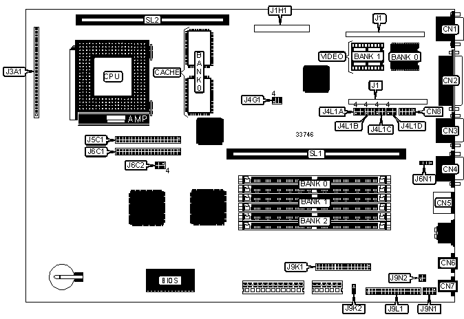
CONNECTIONS | |||
|
Purpose |
Location |
Purpose |
Location |
|
VGA port |
CN1 |
Front panel power switch |
J3A1 pins 14 - 18 |
|
Parallel port |
CN2 |
IR connector |
J3A1 pins 19 - 25 |
|
Serial port 2/USB connector |
CN3 |
Speaker |
J3A1 pins 26 - 29 |
|
Serial port 1 |
CN4 |
IDE interface |
J5C1 |
|
PS/2 mouse port |
CN5 |
IDE interface |
J6C1 |
|
Microphone in connector |
CN6 |
CD-ROM connector |
J6N1 |
|
Audio out connector |
CN7 |
Floppy drive interface |
J9K1 |
|
Serial port 2 |
CN8 |
Power supply remote connector |
J9K2 |
|
ATI media connector |
J1H1 |
MIDI/audio connector |
J9L1 |
|
Chassis fan power |
J3A1 pins 1 - 3 |
Wavetable connector |
J9N1 |
|
Reset switch |
J3A1 pins 4 & 5 |
Telephony connector |
J9N2 |
|
Power LED & keylock |
J3A1 pins 6 - 9 |
Riser slot |
SL1 |
|
IDE interface LED |
J3A1 pins 10 - 13 |
Cache slot |
SL2 |
|
Note: If CN3 is a serial port, CN8 is not present. | |||
|
USER CONFIGURABLE SETTINGS | |||
|
Function |
Label |
Position | |
|
» |
CMOS memory normal operation |
J4L1A |
Pins 4 & 5 closed |
|
CMOS memory clear |
J4L1A |
Pins 5 & 6 closed | |
|
» |
Password enabled |
J4L1A |
Pins 1 & 2 closed |
|
Password disabled |
J4L1A |
Pins 2 & 3 closed | |
|
» |
Setup access enabled |
J4L1B |
Pins 1 & 2 closed |
|
Setup access disabled |
J4L1B |
Pins 2 & 3 closed | |
|
» |
Flash BIOS normal operation |
J6C2 |
Pins 1 & 2 closed |
|
Flash BIOS recovery mode |
J6C2 |
Pins 2 & 3 closed | |
|
DRAM CONFIGURATION | |||
|
Size |
Bank 0 |
Bank 1 |
Bank 2 |
|
8MB |
(2) 1M x 36 |
None |
None |
|
16MB |
(2) 1M x 36 |
(2) 1M x 36 |
None |
|
16MB |
(2) 2M x 36 |
None |
None |
|
24MB |
(2) 2M x 36 |
(2) 1M x 36 |
None |
|
24MB |
(2) 1M x 36 |
(2) 1M x 36 |
(2) 1M x 36 |
|
32MB |
(2) 4M x 36 |
None |
None |
|
32MB |
(2) 2M x 36 |
(2) 2M x 36 |
None |
|
40MB |
(2) 4M x 36 |
(2) 1M x 36 |
None |
|
48MB |
(2) 4M x 36 |
(2) 2M x 36 |
None |
|
48MB |
(2) 4M x 36 |
(2) 1M x 36 |
(2) 1M x 36 |
|
64MB |
(2) 8M x 36 |
None |
None |
|
64MB |
(2) 4M x 36 |
(2) 4M x 36 |
None |
|
80MB |
(2) 8M x 36 |
(2) 2M x 36 |
None |
|
DRAM CONFIGURATION (CON’T) | |||
|
Size |
Bank 0 |
Bank 1 |
Bank 2 |
|
80MB |
(2) 8M x 36 |
(2) 1M x 36 |
(2) 1M x 36 |
|
88MB |
(2) 8M x 36 |
(2) 2M x 36 |
(2) 1M x 36 |
|
96MB |
(2) 8M x 36 |
(2) 4M x 36 |
None |
|
96MB |
(2) 4M x 36 |
(2) 4M x 36 |
(2) 4M x 36 |
|
96MB |
(2) 8M x 36 |
(2) 2M x 36 |
(2) 2M x 36 |
|
128MB |
(2) 8M x 36 |
(2) 4M x 36 |
(2) 4M x 36 |
|
128MB |
(2) 16M x 36 |
None |
None |
|
128MB |
(2) 8M x 36 |
(2) 8M x 36 |
None |
|
136MB |
(2) 16M x 36 |
(2) 1M x 36 |
None |
|
144MB |
(2) 16M x 36 |
(2) 2M x 36 |
None |
|
144MB |
(2) 16M x 36 |
(2) 1M x 36 |
(2) 1M x 36 |
|
152MB |
(2) 16M x 36 |
(2) 2M x 36 |
(2) 1M x 36 |
|
160MB |
(2) 16M x 36 |
(2) 4M x 36 |
None |
|
160MB |
(2) 16M x 36 |
(2) 2M x 36 |
(2) 2M x 36 |
|
176MB |
(2) 16M x 36 |
(2) 4M x 36 |
(2) 2M x 36 |
|
192MB |
(2) 16M x 36 |
(2) 8M x 36 |
None |
|
192MB |
(2) 16M x 36 |
(2) 4M x 36 |
(2) 4M x 36 |
|
200MB |
(2) 16M x 36 |
(2) 8M x 36 |
(2) 1M x 36 |
|
208MB |
(2) 16M x 36 |
(2) 8M x 36 |
(2) 2M x 36 |
|
224MB |
(2) 16M x 36 |
(2) 8M x 36 |
(2) 4M x 36 |
|
256MB |
(2) 32M x 36 |
None |
None |
|
256MB |
(2) 16M x 36 |
(2) 16M x 36 |
None |
|
256MB |
(2) 16M x 36 |
(2) 8M x 36 |
(2) 8M x 36 |
|
264MB |
(2) 16M x 36 |
(2) 16M x 36 |
(2) 1M x 36 |
|
272MB |
(2) 32M x 36 |
(2) 1M x 36 |
(2) 1M x 36 |
|
272MB |
(2) 16M x 36 |
(2) 16M x 36 |
(2) 2M x 36 |
|
288MB |
(2) 32M x 36 |
(2) 2M x 36 |
(2) 2M x 36 |
|
288MB |
(2) 16M x 36 |
(2) 16M x 36 |
(2) 4M x 36 |
|
320MB |
(2) 32M x 36 |
(2) 4M x 36 |
(2) 4M x 36 |
|
320MB |
(2) 16M x 36 |
(2) 16M x 36 |
(2) 8M x 36 |
|
384MB |
(2) 32M x 36 |
(2) 8M x 36 |
(2) 8M x 36 |
|
384MB |
(2) 16M x 36 |
(2) 16M x 36 |
(2) 16M x 36 |
|
512MB |
(2) 32M x 36 |
(2) 32M x 36 |
None |
|
Note: Board accepts EDO memory. Board also accepts x 32 SIMMs. Banks are interchangeable. | |||
|
CACHE CONFIGURATION | ||
|
Size |
Bank 0 |
SL1 |
|
256KB |
(2) 32K x 32 |
Not installed |
|
256KB |
None |
256KB module installed |
|
512KB |
(4) 64K x 8 |
512KB module installed |
|
Note: Either Bank 0 or SL1 will be installed on this board. | ||
|
VIDEO MEMORY CONFIGURATION | |||
|
Size |
Bank 0 |
Bank 1 |
J1 |
|
1MB |
1MB |
None |
Not installed |
|
2MB |
1MB |
(2) 256K x 16 |
Not installed |
|
4MB |
1MB |
(2) 256K x 16 |
2MB module installed |
|
Note: Bank 0 is factory installed and is not configurable. There are 2 sockets for J1. | |||
|
CPU SPEED SELECTION | ||||
|
CPU speed |
Clock speed |
Multiplier |
J4L1C |
J4L1D |
|
75MHz |
50MHz |
1.5x |
2 & 3, 5 & 6 |
1 & 2, 4 & 5 |
|
90MHz |
60MHz |
1.5x |
2 & 3, 4 & 5 |
1 & 2, 4 & 5 |
|
100MHz |
66MHz |
1.5x |
1 & 2, 5 & 6 |
1 & 2, 4 & 5 |
|
120MHz |
60MHz |
2x |
2 & 3, 4 & 5 |
2 & 3, 4 & 5 |
|
133MHz |
66MHz |
2x |
1 & 2, 5 & 6 |
2 & 3, 4 & 5 |
|
150MHz |
60MHz |
2.5x |
2 & 3, 4 & 5 |
2 & 3, 5 & 6 |
|
166MHz |
66MHz |
2.5x |
1 & 2, 5 & 6 |
2 & 3, 5 & 6 |
|
Note: Pins designated should be in the closed position. | ||||
|
CPU TYPE SELECTION | ||
|
Type |
J6C2 | |
| » |
VRE |
Pins 5 & 6 closed |
|
VR |
Pins 4 & 5 closed | |
|
PCI SLOT SELECTION | ||
|
Setting |
J4G1 | |
| » |
Riser card with 2 slots |
Pins 1 & 2, 4 & 5 closed |
|
Riser card with 3 slots |
Pins 2 & 3, 5 & 6 closed | |