IBM CORPORATION
PC 330/350 SERIES (TYPE 65X6)
|
Processor |
Pentium |
|
Processor Speed |
75/90/100MHz |
|
Chip Set |
Unidentified |
|
Video Chip Set |
Unidentified |
|
Maximum Onboard Memory |
128MB |
|
Maximum Video Memory |
2MB |
|
Cache |
256/512KB |
|
BIOS |
Unidentified |
|
Dimensions |
254mm x 218mm |
|
I/O Options |
Floppy drive interface, IDE interfaces (2), parallel port, PS/2 mouse port, serial ports (2), VESA feature connector, VGA port, riser slot |
|
NPU Options |
None |
|
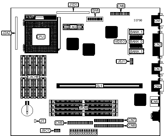
CONNECTIONS | |||
|
Purpose |
Location |
Purpose |
Location |
|
VGA port |
CN1 |
IDE interface |
CN8 |
|
Parallel port |
CN2 |
Floppy drive interface |
CN9 |
|
Serial port |
CN3 |
Voltage regulator |
J1 |
|
Serial port |
CN4 |
Front panel connector |
J1D1 |
|
PS/2 mouse port |
CN5 |
Front panel connector |
J2A2 |
|
VESA feature connector |
CN6 |
Riser slot |
SL1 |
|
IDE interface |
CN7 | ||
|
USER CONFIGURABLE SETTINGS | |||
|
Function |
Label |
Position | |
|
» |
Flash BIOS normal operation |
J5J1 |
Pins 1 & 3 closed |
|
Flash BIOS clear |
J5J1 |
Pins 1 & 2 closed | |
|
» |
Password normal operation |
SW1/3 |
Off |
|
Password clear |
SW1/3 |
On | |
|
» |
CMOS memory normal operation |
SW1/4 |
Off |
|
CMOS memory clear |
SW1/4 |
On | |
|
» |
Factory configured - do not alter |
SW1/5 |
Off |
|
DRAM CONFIGURATION | ||
|
Size |
Bank 0 |
Bank 1 |
|
8MB |
(2) 1M x 36 |
None |
|
16MB |
(2) 2M x 36 |
None |
|
16MB |
(2) 1M x 36 |
(2) 1M x 36 |
|
24MB |
(2) 2M x 36 |
(2) 1M x 36 |
|
32MB |
(2) 4M x 36 |
None |
|
32MB |
(2) 2M x 36 |
(2) 2M x 36 |
|
40MB |
(2) 4M x 36 |
(2) 1M x 36 |
|
48MB |
(2) 4M x 36 |
(2) 2M x 36 |
|
64MB |
(2) 8M x 36 |
None |
|
64MB |
(2) 4M x 36 |
(2) 4M x 36 |
|
72MB |
(2) 8M x 36 |
(2) 1M x 36 |
|
80MB |
(2) 8M x 36 |
(2) 2M x 36 |
|
128MB |
(2) 8M x 36 |
(2) 8M x 36 |
|
Note: Board also accepts x 32 SIMMs. The location of banks 0 & 1 are unidentified. | ||
|
CACHE CONFIGURATION | |||
|
Size |
Bank 0 |
Bank 1 |
TAG |
|
256KB |
(4) 32K x 8 |
(4) 32K x 8 |
(1) 32K x 8 |
|
512KB |
(4) 64K x 8 |
(4) 64K x 8 |
(1) 32K x 8 |
|
Note: The location of banks 0 & 1 are unidentified. | |||
|
CACHE SWITCH CONFIGURATION | ||
|
Size |
SW1/1 |
SW1/2 |
|
None |
On |
N/A |
|
256KB |
Off |
Off |
|
512KB |
Off |
On |
|
VIDEO MEMORY CONFIGURATION | ||
|
Size |
Bank 0 |
Bank 1 |
|
1MB |
1MB |
None |
|
2MB |
1MB |
1MB |
|
Note: Bank 0 is factory installed and is not configurable. The size of the video memory chips are unidentified. | ||
|
CPU SPEED SELECTION | |||||
|
CPU speed |
Clock speed |
Multiplier |
SW1/6 |
SW1/7 |
SW1/8 |
|
75MHz |
50MHz |
1.5x |
Off |
Off |
Off |
|
90MHz |
60MHz |
1.5x |
Off |
On |
Off |
|
100MHz |
66MHz |
1.5x |
Off |
Off |
On |
|
CPU TYPE SELECTION | ||
|
Type |
J9C1 | |
| » |
VR |
Pins 1 & 3 closed |
|
VRE |
Pins 5 & 7 closed | |
|
ISA BUS CLOCK SPEED SELECTION | |||
|
CPU speed |
ISA clock speed |
J5J1 | |
| » |
75MHz (1/6 clock speed) |
8.33MHz |
Pins 5 & 7 open |
|
75MHz (1/8 clock speed) |
6.25MHz |
Pins 5 & 7 closed | |
|
90MHz (1/6 clock speed) |
10MHz |
Pins 5 & 7 open | |
| » |
90MHz (1/8 clock speed) |
7.5MHz |
Pins 5 & 7 closed |
|
100MHz (1/6 clock speed) |
11MHz |
Pins 5 & 7 open | |
|
100MHz (1/8 clock speed) |
8.25MHz |
Pins 5 & 7 closed | |