IBM CORPORATION
APTIVA 2159
|
Processor |
Pentium |
|
Processor Speed |
133/150/166/200MHz |
|
Chip Set |
Unidentified |
|
Video Chip Set |
Unidentified |
|
Maximum Onboard Memory |
128MB (EDO supported) |
|
Maximum Video Memory |
2MB |
|
Cache |
256/512KB |
|
BIOS |
Unidentified |
|
Dimensions |
330mm x 218mm |
|
I/O Options |
Floppy drive interface, IDE interfaces (2), parallel port, PS/2 mouse port, serial port, VESA feature connector, VGA port, VGA interface, riser slot, cache slot, VRM connector, USB connector, Media console connector, wake up on ring connector |
|
NPU Options |
None |
|
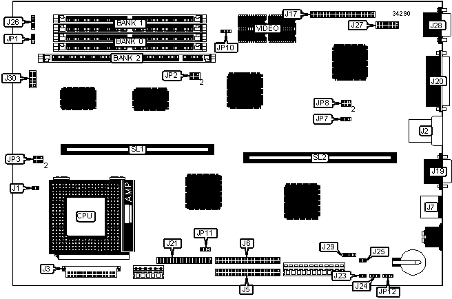
CONNECTIONS | |||
|
Purpose |
Location |
Purpose |
Location |
|
Chassis fan power |
J1 |
Soft off power supply |
J23 |
|
USB connector |
J2 |
Auxiliary 5v connector |
J24 |
|
VRM connector |
J3 |
Wake up on ring connector |
J25 |
|
IDE interface 1 |
J5 |
IDE interface LED |
J26 |
|
IDE interface 2 |
J6 |
VGA interface |
J27 |
|
PS/2 mouse port |
J7 |
VGA port |
J28 |
|
VESA feature connector |
J17 |
Speaker |
J29 |
|
Serial port |
J19 |
Media console connector |
J30 |
|
Parallel port |
J20 |
Cache slot |
SL1 |
|
Floppy drive interface |
J21 |
Riser slot |
SL2 |
|
USER CONFIGURABLE SETTINGS | |||
|
Function |
Label |
Position | |
|
External speaker enabled |
JP1 |
Pins 1 & 2 closed | |
|
External speaker disabled |
JP1 |
Open | |
|
Flash BIOS write protect disabled |
JP7 |
Pins 1 & 2 closed | |
|
Flash BIOS write protect enabled |
JP7 |
Pins 2 & 3 closed | |
|
» |
Factory configured - do not alter |
JP8 |
Unidentified |
|
On board video enabled |
JP10 |
Pins 1 & 2 closed | |
|
On board video disabled |
JP10 |
Pins 2 & 3 closed | |
|
Floppy drive write protect disabled |
JP11 |
Pins 1 & 2 closed | |
|
Floppy drive write protect enabled |
JP11 |
Pins 2 & 3 closed | |
|
» |
CMOS memory normal operation |
JP12 |
Pins 1 & 2 closed |
|
CMOS memory clear |
JP12 |
Pins 2 & 3 closed | |
|
DRAM CONFIGURATION | ||
|
Size |
Bank 0 |
Bank 1 |
|
8MB |
(2) 1M x 36 |
None |
|
16MB |
(2) 2M x 36 |
None |
|
16MB |
(2) 1M x 36 |
(2) 1M x 36 |
|
24MB |
(2) 2M x 36 |
(2) 1M x 36 |
|
32MB |
(2) 4M x 36 |
None |
|
32MB |
(2) 2M x 36 |
(2) 2M x 36 |
|
40MB |
(2) 4M x 36 |
(2) 1M x 36 |
|
48MB |
(2) 4M x 36 |
(2) 2M x 36 |
|
64MB |
(2) 8M x 36 |
None |
|
64MB |
(2) 4M x 36 |
(2) 4M x 36 |
|
72MB |
(2) 8M x 36 |
(2) 1M x 36 |
|
80MB |
(2) 8M x 36 |
(2) 2M x 36 |
|
96MB |
(2) 8M x 36 |
(2) 4M x 36 |
|
128MB |
(2) 8M x 36 |
(2) 8M x 36 |
|
Note: Board accepts EDO memory. Board also accepts x 32 SIMMs. Banks are interchangeable. | ||
|
DIMM CONFIGURATION | |
|
Size |
Bank 0 |
|
8MB |
(1) 1M x 64 |
|
16MB |
(1) 2M x 64 |
|
32MB |
(1) 4M x 64 |
|
64MB |
(1) 8M x 64 |
|
CACHE CONFIGURATION | |
|
Size |
SL1 |
|
256KB |
256KB module installed |
|
512KB |
512KB module installed |
|
VIDEO MEMORY CONFIGURATION |
|
Note: Bank 0 is factory installed with 2MB of video memory and is not configurable. |
|
CPU SPEED SELECTION | ||||
|
CPU speed |
Clock speed |
Multiplier |
JP2 |
JP3 |
|
133MHz |
66MHz |
2x |
1 & 3, 2 & 4 |
2 & 4, 3 & 5 |
|
150MHz |
60MHz |
2.5x |
3 & 5, 4 & 6 |
3 & 5, 4 & 6 |
|
166MHz |
66MHz |
2.5x |
1 & 3, 2 & 4 |
3 & 5, 4 & 6 |
|
200MHz |
66MHz |
3x |
1 & 3, 2 & 4 |
1 & 3, 4 & 6 |
|
Note: Pins designated should be in the closed position. | ||||