MICRO-STAR INTERNATIONAL CO., LTD.
MS-5120
|
Processor |
Pentium |
|
Processor Speed |
75/90/100/120/133MHz |
|
Chip Set |
Intel |
|
Max. Onboard DRAM |
128MB |
|
Cache |
256KB |
|
BIOS |
AMI |
|
Dimensions |
260mm x 220mm |
|
I/O Options |
Parallel port, serial ports (2), IDE interfaces (2), 32-bit PCI slots (3), green PC connector, floppy drive interface, PS/2 mouse connector |
|
NPU Options |
None |
|
CONNECTIONS | |||
|
Purpose |
Location |
Purpose |
Location |
|
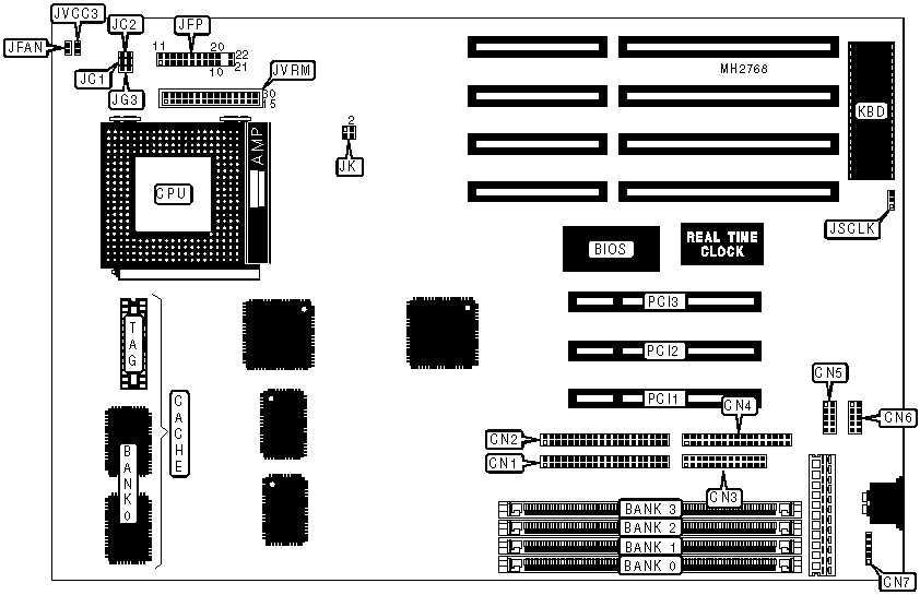
IDE interface (primary) |
CN1 |
Speaker |
JFP pins 7 - 10 |
|
IDE interface (secondary) |
CN2 |
Turbo LED |
JFP pins 12 & 13 |
|
Floppy drive interface |
CN3 |
Turbo switch |
JFP pins 15 - 17 |
|
Parallel port |
CN4 |
Reset switch |
JFP pins 19 & 20 |
|
Serial port 2 |
CN5 |
IDE interface LED |
JFP pins 21 & 22 |
|
Serial port 1 |
CN6 |
Green PC connector |
JG3 |
|
PS/2 Mouse connector |
CN7 |
32-bit PCI slots |
PCI1 - PCI3 |
|
Chassis fan power |
JFAN |
Voltage regulator module |
JVRM |
|
Power LED & keylock |
JFP pins 1 - 5 | ||
|
USER CONFIGURABLE SETTINGS | |||
|
Function |
Jumper |
Position | |
|
» |
PCI bus clock/3 |
JSCLK |
pins 1 & 2 closed |
|
PCI bus clock/4 |
JSCLK |
pins 2 & 3 closed | |
|
DRAM CONFIGURATION | ||||
|
Size |
Bank 0 |
Bank 1 |
Bank 2 |
Bank 3 |
|
4MB |
(1) 1M x 36 |
NONE |
NONE |
NONE |
|
4MB |
NONE |
NONE |
(1) 1M x 36 |
NONE |
|
8MB |
(1) 2M x 36 |
NONE |
NONE |
NONE |
|
8MB |
NONE |
NONE |
(1) 2M x 36 |
NONE |
|
8MB |
(1) 1M x 36 |
(1) 1M x 36 |
NONE |
NONE |
|
8MB |
NONE |
NONE |
(1) 1M x 36 |
(1) 1M x 36 |
|
16MB |
(1) 4M x 36 |
NONE |
NONE |
NONE |
|
16MB |
NONE |
NONE |
(1) 4M x 36 |
NONE |
|
16MB |
(1) 2M x 36 |
(1) 2M x 36 |
NONE |
NONE |
|
16MB |
(1) 1M x 36 |
(1) 1M x 36 |
(1) 1M x 36 |
(1) 1M x 36 |
|
16MB |
NONE |
NONE |
(1) 2M x 36 |
(1) 2M x 36 |
|
24MB |
(1) 1M x 36 |
(1) 1M x 36 |
(1) 2M x 36 |
(1) 2M x 36 |
|
24MB |
(1) 2M x 36 |
(1) 2M x 36 |
(1) 1M x 36 |
(1) 1M x 36 |
|
32MB |
(1) 8M x 36 |
NONE |
NONE |
NONE |
|
32MB |
NONE |
NONE |
(1) 8M x 36 |
NONE |
|
32MB |
(1) 4M x 36 |
(1) 4M x 36 |
NONE |
NONE |
|
32MB |
(1) 2M x 36 |
(1) 2M x 36 |
(1) 2M x 36 |
(1) 2M x 36 |
|
32MB |
NONE |
NONE |
(1) 4M x 36 |
(1) 4M x 36 |
|
40MB |
(1) 1M x 36 |
(1) 1M x 36 |
(1) 4M x 36 |
(1) 4M x 36 |
|
40MB |
(1) 4M x 36 |
(1) 4M x 36 |
(1) 1M x 36 |
(1) 1M x 36 |
|
48MB |
(1) 4M x 36 |
(1) 4M x 36 |
(1) 2M x 36 |
(1) 2M x 36 |
|
48MB |
(1) 2M x 36 |
(1) 2M x 36 |
(1) 4M x 36 |
(1) 4M x 36 |
|
64MB |
(1) 16M x 36 |
NONE |
NONE |
NONE |
|
64MB |
NONE |
NONE |
(1) 16M x 36 |
NONE |
|
64MB |
(1) 8M x 36 |
(1) 8M x 36 |
NONE |
NONE |
|
64MB |
(1) 4M x 36 |
(1) 4M x 36 |
(1) 4M x 36 |
(1) 4M x 36 |
|
64MB |
NONE |
NONE |
(1) 8M x 36 |
(1) 8M x 36 |
|
72MB |
(1) 1M x 36 |
(1) 1M x 36 |
(1) 8M x 36 |
(1) 8M x 36 |
|
72MB |
(1) 8M x 36 |
(1) 8M x 36 |
(1) 1M x 36 |
(1) 1M x 36 |
|
80MB |
(1) 2M x 36 |
(1) 2M x 36 |
(1) 8M x 36 |
(1) 8M x 36 |
|
80MB |
(1) 8M x 36 |
(1) 8M x 36 |
(1) 2M x 36 |
(1) 2M x 36 |
|
96MB |
(1) 4M x 36 |
(1) 4M x 36 |
(1) 8M x 36 |
(1) 8M x 36 |
|
96MB |
(1) 8M x 36 |
(1) 8M x 36 |
(1) 4M x 36 |
(1) 4M x 36 |
|
128MB |
(1) 32M x 36 |
NONE |
NONE |
NONE |
|
128MB |
NONE |
NONE |
(1) 32M x 36 |
NONE |
|
128MB |
(1) 16M x 36 |
(1) 16M x 36 |
NONE |
NONE |
|
128MB |
(1) 8M x 36 |
(1) 8M x 36 |
(1) 8M x 36 |
(1) 8M x 36 |
|
128MB |
NONE |
NONE |
(1) 16M x 36 |
(1) 16M x 36 |
|
CACHE CONFIGURATION |
|
Note: Cache is factory installed and not configurable. |
|
CPU SPEED CONFIGURATION | |
|
Speed |
JK |
|
75MHz |
pins 1 & 3, 2 & 4 closed |
|
90MHz |
pins 1 & 3 closed |
|
100MHz |
pins 2 & 4 closed |
|
120MHz |
pins 1 & 3 closed |
|
133MHz |
pins 2 & 4 closed |
|
CPU VOLTAGE CONFIGURATION | |
|
Voltage |
JVCC3 |
|
3.4v |
Closed |
|
3.5v |
Open |
|
BUS/CORE RATIO CONFIGURATION | |||
|
P54C/CQS/CS |
P54CS POR(C-step) |
JC1 |
JC2 |
|
2/3 |
2/3 |
Open |
Open |
|
1/2 |
1/2 |
Closed |
Open |
|
1/3 |
1/3 |
Open |
Closed |
|
1/4 |
2/5 |
Closed |
Closed |
|
VOLTAGE REGULATOR MODULE PIN IDENTIFICATION | |||
|
Pin |
Purpose |
Pin |
Purpose |
|
1 |
VSS |
16 |
VSS |
|
2 |
VSS |
17 |
VSS |
|
3 |
ND |
18 |
V/IO |
|
4 |
V/IO |
19 |
V/IO |
|
5 |
3.3v |
20 |
3.3v |
|
6 |
3.3v |
21 |
3.3v |
|
7 |
VCORE |
22 |
VCORE |
|
8 |
VCORE |
23 |
VCORE |
|
9 |
VSS |
24 |
VCORE |
|
10 |
VCORE |
25 |
VCORE |
|
11 |
PRGOOD |
26 |
UPVRM# |
|
12 |
SENSE |
27 |
DISABLE |
|
13 |
VSS |
28 |
VSS |
|
14 |
5v |
29 |
5v |
|
15 |
5v |
30 |
5v |
|
Note: The purpose of the Voltage Regulator Module is to allow different voltage processors to be supported by the motherboard. | |||