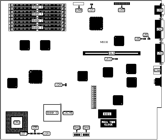
OLIVETTI
LSX5015 (BA305/BA322/BA360/BA365)
LSX5025 (BA306/BA322/BA361)
|
Processor |
80486SX/ODP486SX/80487SX/80486DX/80486DX2 (5015) 80486DX/ODP486DX/80486DX2 (5025) |
|
Processor Speed |
25/50(internal)MHz (5015) 33/66(internal)MHz (5025) |
|
Chip Set |
Unidentified |
|
Video Chip Set |
ET |
|
Maximum Onboard Memory |
64MB |
|
Maximum Video Memory |
None |
|
Cache |
128KB (only on 5025) |
|
BIOS |
Unidentified |
|
Dimensions |
355mm x 304mm |
|
I/O Options |
Parallel port, PS/2 mouse port, serial port, feature connector, VGA port, riser slot |
|
NPU Options |
None |

|
CONNECTIONS | |||
|
Function |
Label |
Function |
Label |
|
VGA port |
CN1 |
Feature connector |
CN5 |
|
Serial port |
CN2 |
Console connector |
CN6 |
|
Parallel port |
CN3 |
Riser slot |
SL1 |
|
PS/2 mouse port |
CN4 | ||
|
USER CONFIGURABLE SETTINGS | |||
|
Setting |
Label |
Position | |
|
» |
Factory configured - do not alter |
J13 |
Open |
|
Temperature sensor enabled |
J21 |
Closed | |
|
Temperature sensor disabled |
J21 |
Open | |
|
DSM board installed |
J24 |
Open | |
|
DSM board not installed |
J24 |
Closed | |
|
» |
PST gate array disabled |
J27 |
Open |
|
PST gate array enabled |
J27 |
Closed | |
|
» |
Serial port chip enabled |
SW1/1 |
On |
|
Serial port chip disabled |
SW1/1 |
Off | |
|
» |
EISA bus on riser board enabled |
SW1/2 |
Off |
|
EISA bus on riser board disabled |
SW1/2 |
On | |
|
» |
Factory configured - do not alter |
SW2/1 |
N/A |
|
» |
Password normal operation |
SW2/2 |
On |
|
Reboots system ignoring CMOS and EISA configuration |
SW2/2 |
Off | |
|
» |
Factory configured - do not alter |
SW2/3 |
N/A |
|
» |
Factory configured - do not alter |
SW2/4 |
N/A |
|
Note: Jumper J27 may not be present on all boards. It is not present on level 2 boards BA305, BA360 & BA365 and level 1 boards BA306 & BA361. | |||
|
DRAM CONFIGURATION | ||||
|
Size |
Bank 0 |
Bank 1 |
Bank 2 |
Bank 3 |
|
4MB |
(2) 512K x 36 |
None |
None |
None |
|
8MB |
(2) 512K x 36 |
(2) 512K x 36 |
None |
None |
|
8MB |
(2) 1M x 36 |
None |
None |
None |
|
12MB |
(2) 512K x 36 |
(2) 512K x 36 |
(2) 512K x 36 |
None |
|
12MB |
(2) 1M x 36 |
None |
(2) 512K x 36 |
None |
|
16MB |
(2) 512K x 36 |
(2) 512K x 36 |
(2) 512K x 36 |
(2) 512K x 36 |
|
16MB |
(2) 1M x 36 |
None |
(2) 512K x 36 |
(2) 512K x 36 |
|
16MB |
(2) 1M x 36 |
(2) 1M x 36 |
None |
None |
|
16MB |
(2) 2M x 36 |
None |
None |
None |
|
20MB |
(2) 1M x 36 |
(2) 1M x 36 |
(2) 512K x 36 |
None |
|
20MB |
(2) 2M x 36 |
None |
(2) 512K x 36 |
None |
|
24MB |
(2) 1M x 36 |
(2) 1M x 36 |
(2) 512K x 36 |
(2) 512K x 36 |
|
24MB |
(2) 2M x 36 |
(2) 1M x 36 |
(2) 1M x 36 |
None |
|
DRAM CONFIGURATION (CON’T) | ||||
|
Size |
Bank 0 |
Bank 1 |
Bank 2 |
Bank 3 |
|
24MB |
(2) 2M x 36 |
None |
(2) 512K x 36 |
(2) 512K x 36 |
|
24MB |
(2) 2M x 36 |
None |
(2) 1M x 36 |
None |
|
32MB |
(2) 1M x 36 |
(2) 1M x 36 |
(2) 1M x 36 |
(2) 1M x 36 |
|
32MB (UNIX) |
(2) 2M x 36 |
None |
(2) 1M x 36 |
(2) 1M x 36 |
|
32MB (DOS) |
(2) 1M x 36 |
(2) 1M x 36 |
(2) 2M x 36 |
None |
|
32MB |
(2) 2M x 36 |
(2) 2M x 36 |
None |
None |
|
36MB |
(2) 2M x 36 |
(2) 2M x 36 |
(2) 512K x 36 |
None |
|
40MB |
(2) 2M x 36 |
(2) 2M x 36 |
(2) 512K x 36 |
(2) 512K x 36 |
|
40MB |
(2) 2M x 36 |
(2) 2M x 36 |
(2) 1M x 36 |
None |
|
48MB |
(2) 2M x 36 |
(2) 2M x 36 |
(2) 1M x 36 |
(2) 1M x 36 |
|
48MB |
(2) 2M x 36 |
(2) 2M x 36 |
(2) 2M x 36 |
None |
|
64MB |
(2) 2M x 36 |
(2) 2M x 36 |
(2) 2M x 36 |
(2) 2M x 36 |
|
CACHE CONFIGURATION | |
|
Size |
Bank 0 |
|
128KB |
128KB |
|
Note: Cache upgrade socket is only on the 5025 mainboard. | |
|
CPU SPEED SELECTION (5015) | ||
|
Speed |
SW1/3 |
SW1/4 |
|
25MHz (5015) |
Off |
On |
|
50iMHz (5015) |
Off |
On |
|
CPU SPEED SELECTION (5025) | ||
|
Speed |
SW1/3 |
SW1/4 |
|
33MHz (5025) |
On |
Off |
|
66iMHz (5025) |
On |
Off |
|
CPU TYPE SELECTION (5015) | ||
|
Type |
J25 |
J26 |
|
80486SX |
Open |
Closed |
|
ODP486SX |
Open |
Open |
|
80487SX |
Open |
Open |
|
80486DX |
Closed |
Open |
|
80486DX2 |
Closed |
Open |
|
CPU TYPE SELECTION (5025) | ||
|
Type |
J25 |
J26 |
|
80486DX |
Closed |
Open |
|
ODP486DX |
Open |
Open |
|
80486DX2 |
Closed |
Open |
|
SERIAL PORT MODE SELECTION | |||
|
Setting |
J6 |
J8 | |
| » |
Enabled in Fail Safe Mode |
Closed |
Closed |
|
Enabled in AT mode |
Open |
Open | |
|
MISCELLANEOUS TECHNICAL NOTE |
|
The location of pin 1 on CN5 is unidentified. |