WYSE TECHNOLOGY, INC.
WYSE PC 386 MODEL 3216
|
Processor |
80386DX |
|
Processor Speed |
16MHz |
|
Chip Set |
WYSE |
|
Max. Onboard DRAM |
None |
|
Cache |
None |
|
BIOS |
WYSE |
|
Dimensions |
334mm x 122mm |
|
I/O Options |
Proprietary top plane local bus connector |
|
NPU Options |
80287/80387 |
|
CONNECTIONS |
|||
|
Purpose |
Location |
Purpose |
Location |
|
Reset |
J1 |
Power good/Speaker |
J4 |
|
Keylock |
J2 |
Local bus card edge connector |
S1 |
|
External battery |
J3 |
|
|
|
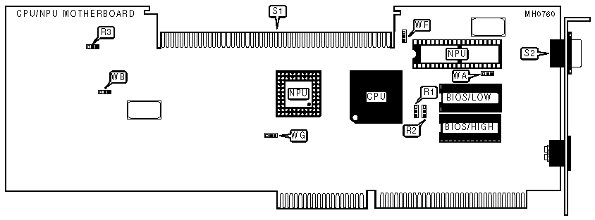
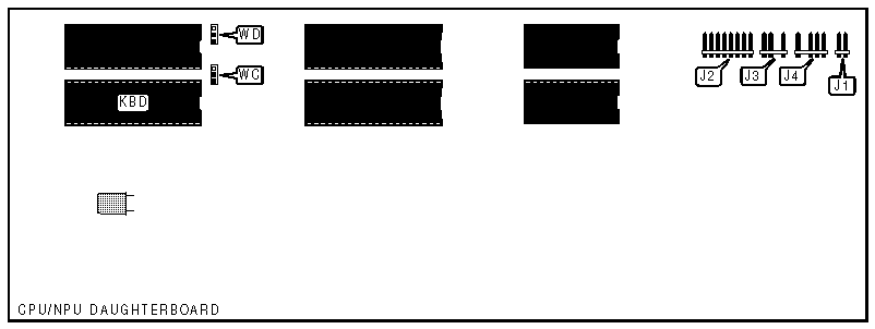
USER CONFIGURABLE SETTINGS ON THE CPU/NPU BOARDS |
|||
|
Function |
Jumper |
Position |
|
|
» |
Factory configured - do not alter |
R3 |
pins 2 & 3 closed |
|
» |
NPU disabled |
WB |
pins 2 & 3 closed |
|
|
NPU enabled |
WB |
pins 1 & 2 closed |
|
» |
Factory test disabled |
WC |
pins 1 & 2 closed |
|
|
Factory test enabled |
WC |
pins 2 & 3 closed |
|
» |
Monitor type select color |
WD |
pins 1 & 2 closed |
|
|
Monitor type select monochrome |
WD |
pins 2 & 3 closed |
|
» |
Factory configured - do not alter |
WF |
pins 1 & 2 closed |
|
BIOS CONFIGURATION |
||
|
Size |
R1 |
R2 |
|
27128 |
pins 2 & 3 closed |
pins 1 & 2 closed |
|
27256 |
pins 1 & 2 closed |
pins 1 & 2 closed |
|
27512 |
pins 1 & 2 closed |
pins 2 & 3 closed |
|
NPU CONFIGURATION |
||
|
Type |
WA |
WG |
|
80287 |
pins 1 & 2 closed |
pins 2 & 3 closed |
|
80387 |
pins 2 & 3 closed |
pins 1 & 2 closed |
|
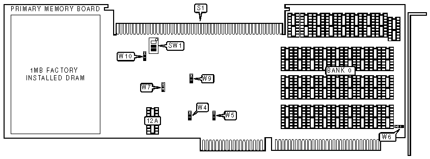
PRIMARY MEMORY BOARD DRAM JUMPER CONFIGURATION |
||||||
|
Size |
W4 |
W5 |
W6 |
W7 |
W9 |
W10 |
|
1MB |
1 & 2 |
1 & 2 |
2 & 3 |
1 & 2 |
1 & 2 |
1 & 2 |
|
2MB 1 |
2 & 3 |
2 & 3 |
2 & 3 |
2 & 3 |
2 & 3 |
2 & 3 |
|
Note:Pins designated should be in the closed position. Note 1 :To achieve 2MB on the Primary Memory Board, populate Bank 0 with (36) 41256 DRAM chips. |
||||||
|
PRIMARY MEMORY BOARD DRAM SWITCH CONFIGURATION |
|||
|
Configuration with a PAL 250451-01 chip installed at location 12A |
|||
|
Size |
SW1/1 |
SW1/2 |
SW1/3 |
|
1MB |
On |
Off |
Off |
|
2MB |
On |
Off |
Off |
|
4MB 1 |
Off |
On |
Off |
|
6MB 2 |
On |
On |
Off |
|
Configuration with a PAL 250358-01 chip installed at location 12A |
|||
|
1MB |
On |
On |
On |
|
2MB |
On |
On |
On |
|
4MB 1 |
On |
On |
Off |
|
6MB 2 |
On |
On |
Off |
|
Note:Either 1MBor 2MB may be configured on the Primary Memory Board. Note 1 :Memory configuration of 4MB is possible with the installation of one additional memory board. Note 2 :Memory configuration of 6MB is possible with the installation of two additional memory boards. |
|||
|
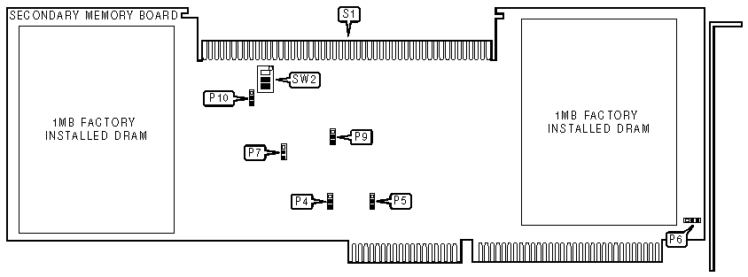
USER CONFIGURABLE SETTINGS ON THE ADDITIONAL MEMORY BOARDS |
|||
|
Function |
Switch |
Position |
|
|
» |
Factory configured - do not alter |
P4 |
pins 2 & 3 closed |
|
» |
Factory configured - do not alter |
P5 |
pins 2 & 3 closed |
|
» |
Factory configured - do not alter |
P6 |
pins 2 & 3 closed |
|
» |
Factory configured - do not alter |
P7 |
pins 2 & 3 closed |
|
» |
Factory configured - do not alter |
P9 |
pins 2 & 3 closed |
|
» |
Factory configured - do not alter |
P10 |
pins 2 & 3 closed |
|
MEMORY BOARD SWITCH CONFIGURATION |
|||
|
Size |
SW2/1 |
sw2/2 |
sw2/3 |
|
Additional Memory Board configured as the second memory board (the Primary Memory Board must be installed first) |
Off |
Off |
Off |
|
Additional Memory Board configured as the third memory board (the Primary Memory Board, and one other Additional Memory Board must be installed first) |
On |
Off |
Off |