UNIDENTIFIED
80286 MOTHER BOARD
|
Processor |
80286 |
|
Processor Speed |
12/25MHz |
|
Chip Set |
Suntac |
|
Max. Onboard DRAM |
4MB |
|
Cache |
Award/Phoenix |
|
BIOS |
Unidentified |
|
Dimensions |
330mm x 218mm |
|
I/O Options |
None |
|
NPU Options |
80287 |
|
CONNECTIONS | |||
|
Purpose |
Location |
Purpose |
Location |
|
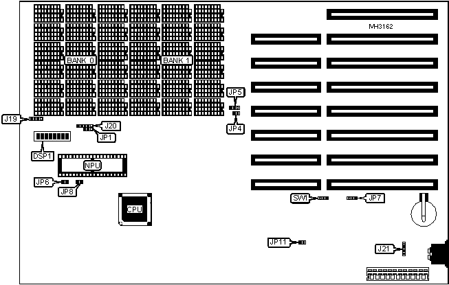
Speaker |
J19 |
Turbo LED |
JP5 |
|
Power LED & keylock |
J20 |
Reset switch |
JP6 |
|
External battery |
J21 | ||
|
USER CONFIGURABLE SETTINGS | |||
|
Function |
Jumper/Switch |
Position | |
|
» |
Factory configured - do not alter |
DSP1/2 |
N/A |
|
» |
Factory configured - do not alter |
DSP1/4 |
N/A |
|
» |
Factory configured - do not alter |
J18 |
pins 2 & 3 closed |
|
BIOS type select Award |
JP7 |
pins 2 & 3 closed | |
|
BIOS type select Phoenix |
JP7 |
pins 1 & 2 closed | |
|
Memory wait state select 0 wait states |
JP11 |
Closed | |
|
Memory wait state select 1 wait state |
JP11 |
Open | |
|
Monitor type select color |
SW1 |
pins 2 & 3 closed | |
|
Monitor type select monochrome |
SW1 |
pins 1 & 2 closed | |
|
Note: The location of J18 is unidentified. | |||
|
DRAM CONFIGURATION | |||||
|
Mode |
Size |
Base memory |
EMS |
Bank 0 |
Bank 1 |
|
0 |
512KB |
512KB |
N/A |
(18) 41256 |
NONE |
|
1 |
640KB |
640KB |
N/A |
(18) 41256 |
(18) 4164 |
|
2 |
1MB |
1MB |
N/A |
(18) 41256 |
(18) 41256 |
|
3 |
1MB |
640KB |
384KB |
(18) 41256 |
(18) 41256 |
|
4 |
2MB |
2MB |
N/A |
(18) 411000 |
NONE |
|
5 |
2MB |
640KB |
1408KB |
(18) 411000 |
NONE |
|
6 |
4MB |
4MB |
N/A |
(18) 411000 |
(18) 411000 |
|
7 |
4MB |
640KB |
3456KB |
(18) 411000 |
(18) 411000 |
|
DRAM SWITCH CONFIGURATION | |||
|
Mode |
DSP1/6 |
DSP1/7 |
DSP1/8 |
|
0 |
On |
On |
On |
|
1 |
On |
On |
Off |
|
2 |
On |
Off |
On |
|
3 |
On |
Off |
Off |
|
4 |
Off |
On |
On |
|
5 |
Off |
On |
Off |
|
6 |
Off |
Off |
On |
|
7 |
Off |
Off |
Off |
|
DRAM MODE CONFIGURATION | |
|
Setting |
JP8 |
|
Mode changes external |
Closed |
|
Mode changes internal |
Open |
|
CLOCK SPEED CONFIGURATION | |||
|
Setting |
DSP1/1 |
JP1 |
JP4 |
|
High speed (internal) |
Off |
pins 2 & 3 closed |
N/A |
|
Low speed (internal) |
On |
pins 2 & 3 closed |
N/A |
|
High speed (external) |
N/A |
pins 1 & 2 closed |
Closed |
|
Low speed (external) |
N/A |
pins 1 & 2 closed |
Open |
|
Note: If JP4 is open, speed can be switched through the keyboard. High speed: CNTL, ALT, 2. Low speed: CNTL, ALT, 1. (Award BIOS only) | |||
|
I/O WAIT STATE CONFIGURATION | ||
|
Wait states |
JP3 |
DSP1/3 |
|
4 |
pins 2 & 3 closed |
On |
|
6 |
pins 2 & 3 closed |
Off |
|
6 |
pins 1 & 2 closed |
N/A |
|
Note: The location of JP3 is unidentified. | ||
|
BIOS CONFIGURATION | ||
|
Type |
JP9 |
DSP1/5 |
|
27128 |
pins 1 & 2 closed |
On |
|
27256 |
pins 2 & 3 closed |
Off |
|
Note: The location of JP9 is unidentified. | ||