UNIDENTIFIED
VCW33 REV:B
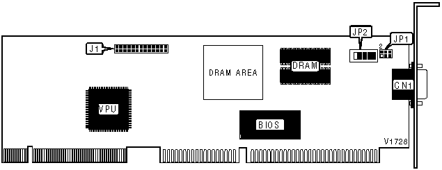
|
Card Type |
Video |
|
Chip Set |
Western Digital |
|
Maximum Onboard Memory |
2MB DRAM |
|
Data Bus |
32-bit VESA Local Bus |
|
Video Types Supported |
XVGA |
|
Highest Resolution Supported |
1280 x 1024 |
|
CONNECTIONS | |||
|
Function |
Label |
Function |
Label |
|
15-pin analog video port |
CN1 |
Feature connector |
J1 |
|
USER CONFIGURABLE SETTINGS | |||
|
Setting |
Label |
Position | |
|
Standard modes at 60Hz |
JP1/pins 1 & 2 |
Open | |
|
Standard modes at 72Hz |
JP1/pins 1 & 2 |
Closed | |
|
Local BUS timing 1 |
JP1/pins 3 & 4 |
Open | |
|
Local BUS timing 2 |
JP1/pins 3 & 4 |
Unidenitified | |
| » |
Factory configured - do not alter |
JP1/pins 5 & 6 |
N/A |
| » |
Standard font |
JP2/5 |
Off |
|
TUV font |
JP2/5 |
On | |
|
MONITOR RETRACE TIMING (800 X 600) | ||||
|
Vertical |
Horizontal |
JP2/1 |
JP2/2 | |
| » |
56Hz (Non interlace) |
35KHz |
Off |
Off |
|
56Hz (Non interlace) |
35KHz |
On |
On | |
|
60Hz (Non interlace) |
47KHz |
Off |
On | |
|
72Hz (Non interlace) |
37KHz |
On |
Off | |
|
MONITOR RETRACE TIMING (1024 X 768) | ||||
|
Vertical |
Horizontal |
JP2/3 |
JP2/4 | |
| » |
87Hz (Non interlace) |
35KHz |
Off |
Off |
|
60Hz (Non interlace) |
48KHz |
Off |
On | |
|
70Hz (Non interlace) |
56KHz |
On |
Off | |
|
72Hz (Non interlace) |
59KHz |
On |
On | |
|
MISCELLANEOUS TECHNICAL NOTE |
|
The "DRAM Area" is populated with (8) 256K x 4 chips but the exact configuration of the chips is unidentified. |